Semiconductor Definition: Semiconductors are elements which have a conductivity between conductors and insulators. Semiconductors can be pure materials, such as silicon or germanium, or a combination of different materials such as gallium arsenide or cadmium selenide.
In a doping technique, impurities are added to pure semiconductors making changes in the material conductivity.
Semiconductors Basics
The study of semiconductors, transistors, and integrated circuits requires an understanding of new concepts in electronic theory. Let’s review what we have learned about conductors.
- Copper and several other metals, such as silver and gold, make good conductors.
- Certain materials, such as glass and rubber, are insulators.
- Semiconductors are composed of materials that are neither good conductors nor good insulators. Semiconductor diodes, transistors, and integrated circuits are all made of semiconductors. Their materials are neither good conductors nor good insulators.
However, the ability of these devices to conduct electricity or to insulate can be greatly enhanced. It will be necessary to take a deeper look at the atomic structure of materials to fully grasp the theory of semiconductor operation.
Atomic Characteristics
Diagrams of the atomic structures of silicon (Si) and germanium (Ge) are shown in Figure 1. Silicon is in great supply. It makes up 28 percent of the world’s surface. The atomic number for silicon is 14. The atomic number of germanium is 32.
Recall that the atomic number is the number of protons or electrons that make up an atom of that element. Therefore, silicon has 14 electrons in its orbit. Germanium has 32 electrons in its orbit.
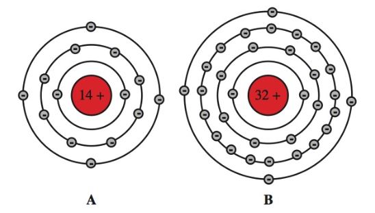
Figure 1. Atomic structures
A–Silicon has an atomic number of 14. There are 14 protons within the nucleus and 14 electrons orbiting the nucleus.
B–Germanium has an atomic number of 32. There are 32 protons in the nucleus and 32 electrons orbiting the nucleus.
Note that both silicon and germanium have four electrons in their outer rings. These electrons on the outer rings are called valence electrons.
In some atoms, valence electrons are able to bond with the valence electrons of another atom. This is called a covalent bond.
The atoms are each bonded to their own nucleus and to each other. This bond creates a lattice crystalline structure. Germanium and silicon both lend themselves to this type of bond. Figure 2 shows a silicon structure. It is a pure insulator. It will not conduct electricity.
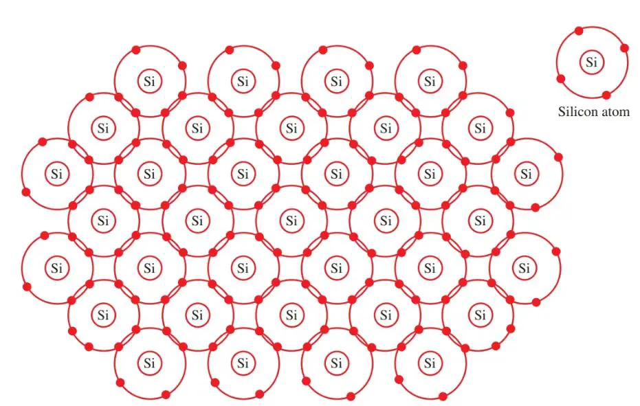
Figure 2. Silicon atoms form covalent bonds. This produces a lattice crystalline structure.
Conduction of Electricity
Electrical current is best defined as the flow of electrons in a conductor.
The flow of electrons results in energy. An example of this action is shown in Figure 3. An electron is added to one end of the conductor. Another electron leaves the opposite end. This chain reaction is the conduction of electricity by electrons.
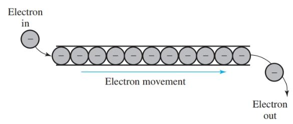
Figure 3. Electricity conducted by the movement of electrons.
In Figure 4, an electron is removed from one end of the conductor. This action leaves a hole where there should be an electron, but there is not.
The hole is strongly attracted to another electron. The hole is positive. The next electron fills up the hole and leaves a positive hole in its place.
Each positive hole is filled in turn by the next electron. Then the vacant hole appears at the other end of the conductor. This chain reaction is the conduction of electricity by holes. The study of semiconductors is concerned with conduction by electrons and by holes.
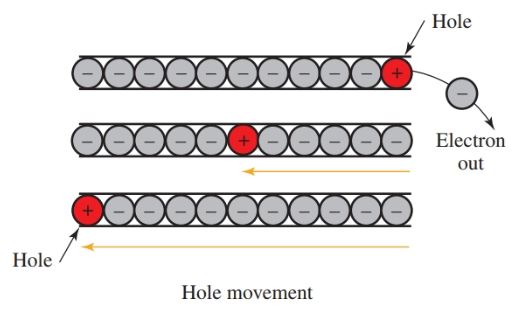
Figure 4. Electricity conducted by the movement of holes.
Doping
Recall that pure silicon is a good insulator. Adding an impurity to the pure silicon changes the conduction traits of the material.
The process of adding impurities to pure semiconductor material is called doping.
The result of doping is an extrinsic semiconductor. This means the material is not in its pure form. A pure semiconductor is intrinsic.
Trivalent and pentavalent impurities are most often used for doping in transistors. Trivalent impurities have three valence electrons. Pentavalent impurities have five valence electrons. Figure 5 is a chart showing the number of valence electrons in several materials.
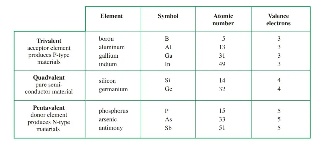
Figure 5. Comparison of trivalent, quad valent, and pentavalent elements. Quad valent elements are pure semiconductors.
Adding doping elements to semiconductor material results in either an excess or shortage of electrons in the covalent bond. For example, arsenic, which is a pentavalent (five electrons in its outer shell), is added to silicon.
Four valence electrons of arsenic form a covalent bond with the four valence electrons of silicon. One electron from the arsenic remains free, Figure 6. The arsenic donated a free electron to the structure.
All pentavalent impurities donate free electrons. They are called donor impurities. In this structure, electricity is conducted by (negative) electrons. Therefore, the crystal becomes an N-type crystal.
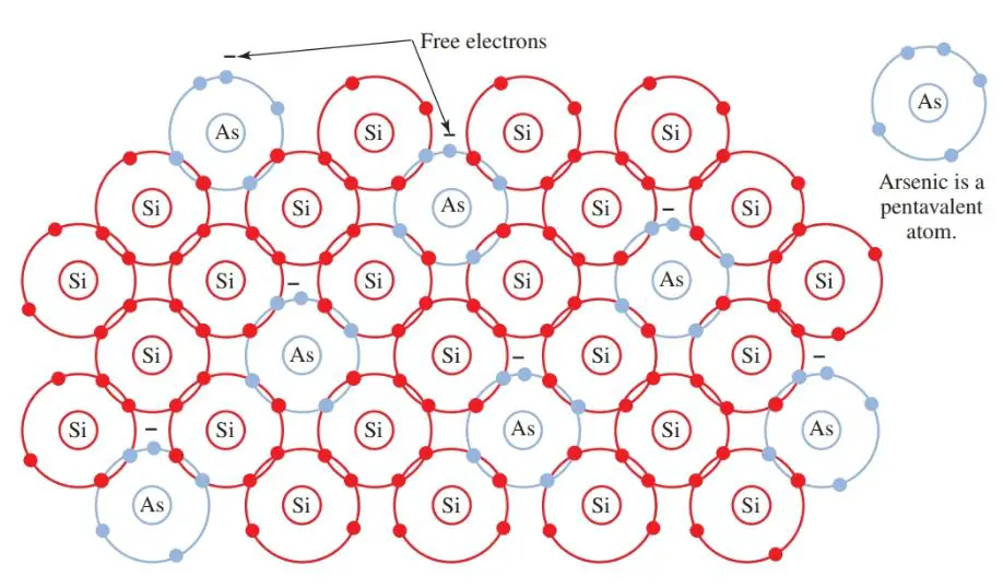
Figure 6. Arsenic (As) is a pentavalent impurity. When combined with a silicon crystal structure, an N-type material is formed.
What occurs when a trivalent impurity is added to a pure semiconductor material?
It has only three electrons to join into a covalent bond. One more electron is needed to complete the lattice structure. A hole remains in the place of the missing electron, Figure 7. This hole will accept an electron.
A trivalent impurity, then, is called an acceptor impurity. In this structure, electricity is conducted by (positive) holes. The crystal becomes a P-type crystal.
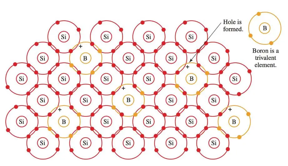
Figure 7. Boron is a trivalent impurity. When boron is combined with a silicon structure, positive holes are created.
Figure 8 shows conduction through an N-type crystal. Figure 9 shows conduction through a P-type crystal. Notice that the hole moves in the opposite direction of the electron flow.
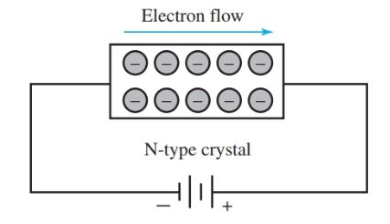
Figure 8. Conduction through an N-type crystal by electrons.
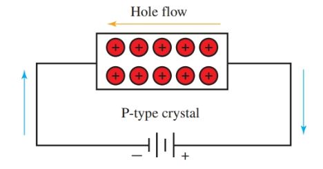
Figure 9. Conduction through a P-type crystal by holes.