The article explains the basics of flip-flops, which are memory elements used in digital electronics for storing binary information. It covers the structure and operation of basic flip-flops, introduces clock-controlled flip-flops, and discusses various types such as J-K, D, and T flip-flops, along with their applications and characteristics. The article also touches on the importance of initialization with preset and clear inputs in flip-flops.
What Is a Flip-Flop in Digital Electronics?
A flip-flop is the basic memory element for storing a bit of information. It is an edge-triggered device. That is, it reacts to the edge of a pulse. A simple flip-flop has two stable states (remember, for instance, that a capacitor has two states: charged and discharged). States are represented by 1 and 0.
Stable state implies that the device remains in one state (e.g., 0) until an input changes its condition to the alternative state. Because a flip-flop has two states only, it is called a bi-stable device.
How a Flip-Flop Works
A basic flip-flop has two inputs and two outputs, as shown in Figure 1. The two inputs are used to set or reset the device and are denoted by R and S. The outputs are denoted by Q and $\overline{Q}$; they reflect the state of the flip-flop either 1 or 0. If Q = 1, then $\overline{Q}$ = 0, and if Q = 0, then and $\overline{Q}$ = 1. Figure 1 illustrates also the truth table for the states of a flip-flop.
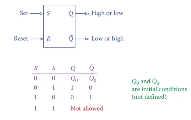
Figure 1 Basic flip-flop.
A flip-flop acts like a single-pole double-throw (SPDT) switch. When activated, it’s output toggles. This property can be used for many operations performed in digital electronics. The toggle action is performed through the inputs to a flip-flop.
There are a few types of flip-flops, as will be described shortly, in terms of their operational properties. The one shown in Figure 1 is the basic flip-flop or the simplest type.
Bi-stable: Having two stable (controllable) states.
Set: (for a flip-flop) Putting a device to the desired state. Some devices have only two states on and off, or high and low. Set implies putting the device in a desired (usually non-default) state.
Reset: Action of putting or setting a device to its default state.
Active level: The (high or low) level in which a logic device functions.
Active low: Implying that the active level for a device is low, as opposed to active high.
Active high: Two-state logic device (e.g., true and false, on and off, high and low) that acts (executes its function) when it is in a high state, as opposed to being active when in the low state.
Before continuing further we need to categorize flip-flops based on their structure, which defines the active level for a flip-flop. Active level is the logic level (high or low) that activates a device. For flip-flops, it implies if a flip-flop is set, or its state toggles, with a logical high or a logical low applied to its set input. In this sense, there are two categories of flip-flops, those whose active level is 1 and those whose active level is 0, i.e., those that are active high and those that are active low.
Types of Flip-Flop
There are a few types of flip-flops in terms of their operational properties:
- Basic Flip-Flop
- Clock-Controlled Flip-Flop
- J-K Flip-Flop
- D Flip-Flop
- T Flip-Flop
Basic Flip-Flop
The basic flip-flop is set by applying an active level signal to its set input and the inverse signal to its reset input. When the unit is set, the Q output is high and the $\overline{Q}$ output is low. If, instead, the active level signal is applied to the reset terminal and its complement is applied to the set terminal, then the $\overline{Q}$ output is high and the Q output is low.
Also, as shown in Figure 1, one cannot apply a logical high to both set and reset of a basic flip-flop at the same time. It is like simultaneously pressing the start and stop button of an electric motor.
Structurally, a flip-flop can be made of two NOR gates or two NAND gates. This is shown in Figure 2. The gates are interconnected to each other or, in other words, they have feedback. The output of each gate is one of the two inputs to the other gate.
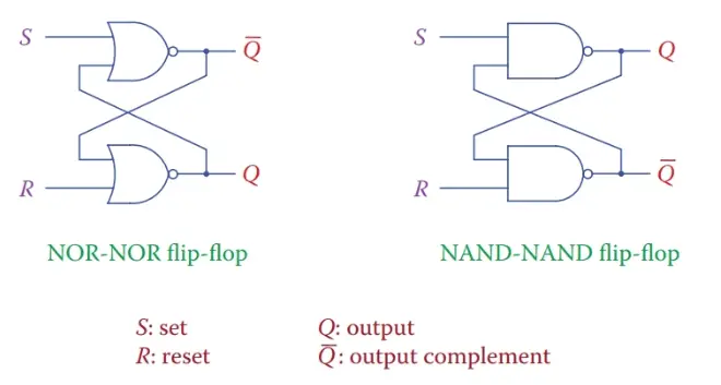
Figure 2 Internal structure of flip-flops.
Note the output of the gate designated as S. For the NOR-NOR flip-flop this is $\overline{Q}$; whereas for the NAND-NAND flip-flop, it is Q. Also, the active level for the former is 1, and for the latter is 0. In both types, a set input sets the content of output Q to high. To change the value of the output to low, the reset must be used. In other words, when the flip-flop is set, if the value of the input set changes to its complement it does not have any effect on the output.
In a NOR-NOR flip-flop the active level is high, but for a NAND- NAND flip-flop it is low.
A flip-flop is either set or it is reset. If it is set, it implies that the set button is activated. In this case, it is meaningless to set it again. Also, it is meaningless to make reset active, too. Thus, to reset a flip-flop, first, the set must be deactivated, and then the reset must be activated. Deactivation takes place by removing (turning off) the input signal.
Likewise, to set a flip-flop after it has been reset, first, the reset must be deactivated (this by itself has no effect and does not change in the status of the output), and then, if set is activated, it sets the flip-flop (it is meaningless to activate set if the reset is still active).
A flip-flop is set by the set input when the reset is not activated. It is reset by reset input when the set is not activated.
Note: In a pushbutton, the activation is performed by pushing, but immediately a spring brings the button to the deactivated position after being released. A flip-flop does not have the spring action; thus, the deactivation has to be separately performed.
What was said above can be observed in Figure 3 for both a NOR-NOR gate and for a NAND-NAND gate. Each gate has two inputs. One of the inputs, being either $\overline{Q}$ or $Q$, reinforces the stability of the output.
Figure 3 also shows that when a flip-flop is set, if S changes, nothing happens, and when it is reset, if R changes, nothing happens.
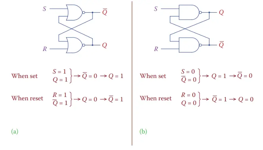
Figure 3 Stability reinforcement in (a) active high and (b) active low flip-flops.
Clock-Controlled Flip-Flops
Clock-controlled flip-flops are more appropriate for synchronized operations, which is the case in microprocessor-controlled systems. The action of a flip-flop takes place with the clock pulse; therefore, it is in synchronism with all other operations (by other flip-flops).
Setting, resetting, or toggling are the three actions of a flip-flop; depending on the inputs one is carried out at either the rising edge of the clock pulse or the falling edge of the clock pulse. This depends on whether a flip-flop is positive edge sensitive or negative edge sensitive. The symbols for the two are depicted in Figure 4.
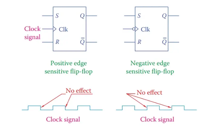
Figure 4 Symbols for positive and negative edge triggering flip-flops.
For the desired action the data for the flip-flop inputs (0 and 1 values) are applied to them before the clock pulse enables the action. The clock input, shown as clk in Figure 4, is sometimes referred to as enable because it enables an action to take place. With the clock pulse, if the set input is activated, the flip-flop sets, and if the reset input is activated, it resets.
Figure 5a indicates how a clock or an enable signal is added to a flip-flop. This is shown only for a NOR-NOR flip-flop, but a NAND-NAND flip-flop has a similar structure. Figure 5 also illustrates how a basic flip-flop can be used with two AND gates in forming a J-K flip-flop.
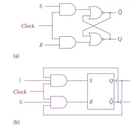
Figure 5 (a) Adding a clock input to a flip-flop and (b) structure of a J-K flip-flop.
J-K Flip-Flop
A J-K flip-flop is clock-controlled and has the advantage that unlike the basic flip-flop it can accept both inputs (now called J and K inputs) to have an active level signal. This combination is prohibited for a basic flip-flop. The effect of having both inputs activated is a toggle of the output state.
In a J-K flip-flop, J input is used as set and K input as reset. When both J and K inputs are active, the flip-flop toggles its output (each output switched to its complementary value, no matter what its current value is). The symbol and the truth table of a J-K flip-flop are shown in Figure 6.
J-K flip-flop: Flip-flop with two data entries, one for set and one for reset the output. It is also possible to toggle the output by activating both inputs.
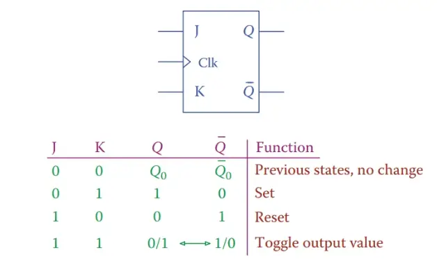
Figure 6 J-K flip-flop.
D Flip-Flop
A data or D flip-flop is a clocked J-K flip-flop that has only one input. The arrangement is as shown in Figure 7a, which indicates how the one output relates to the J and K terminals.
The property of a D flip-flop is that the output follows the input. That is, with the clock pulse, the output will be whatever (0 or 1) has been placed on the input. Figure 7b shows this; even if the input (data) changes at points D1, D2, and so on, the output values update does not occur until the rising edge of the clock pulse, at C1, C2, and C4 (assuming the device is rising edge sensitive).
D flip-flop: A flip-flop with only one input whose output follows the input after the enable or clock signal.
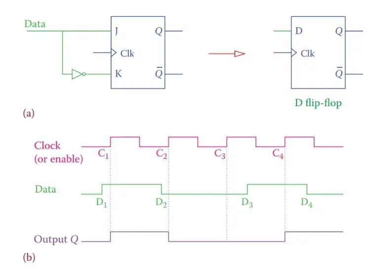
Figure 7 (a) Structure and symbol for D flip-flop. (b) Example of a D flip-flop timing diagram.
T Flip-Flop
Another product based on a J-K flip-flop is a T flip-flop. Similar to D flip-flop it has a clock input and only one data input. If the input is logic 1, then at the active clock pulse edge the output is toggled.
Figure 8 depicts the structure for a T flip-flop and the truth table indicating what happens after the clock signal enable the flip-flop action based on the input and the output state. Note that a T flip-flop is based on a D flip-flop in which Q follows D.
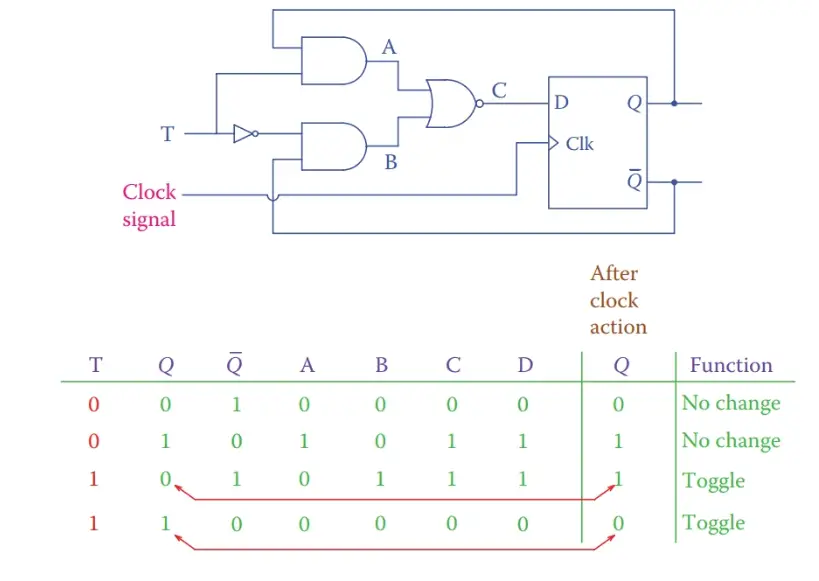
Figure 8 Structure of a T flip-flop.
As we have observed, a J-K flip-flop toggles its output when both J and K inputs are set high. The toggle action takes place with the active edge of the clock pulse. Also, the T flip-flop toggles its output when the T input is high. Again, the action is carried out at the clock pulse edge.
There is another arrangement where a flip-flop toggles with the clock pulse. This is with a D flip-flop as shown in Figure 9, in which the complementary output is fed back to the data input. Because the output must follow the input, as the clock enables the action Q takes the value of $\overline{Q}$, thus toggling. Notice that when a flip-flop toggles, the frequency of its output pulse train is 1/2 of the clock frequency.
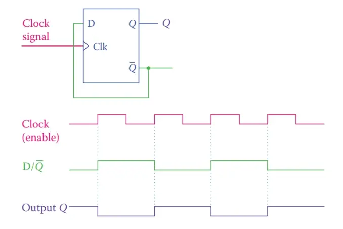
Figure 9 Toggle action with D flip-flop.
Initialization
Normally, when a logic circuit becomes active, for example, at power-up, the initial condition of a flip-flop is not defined or not known. We may need to make sure in what state it is before proceeding with operations. For this reason, two other inputs are added to flip-flops, a preset and a clear.
If the preset is activated it forces the output to go high (Q = 1), and if the clear is activated it forces the output to low (Q = 0). Clear and preset override the clock action. Figure 10 shows the symbol for a D flip-flop with these two entries and a sample timing diagram indicating their effect.
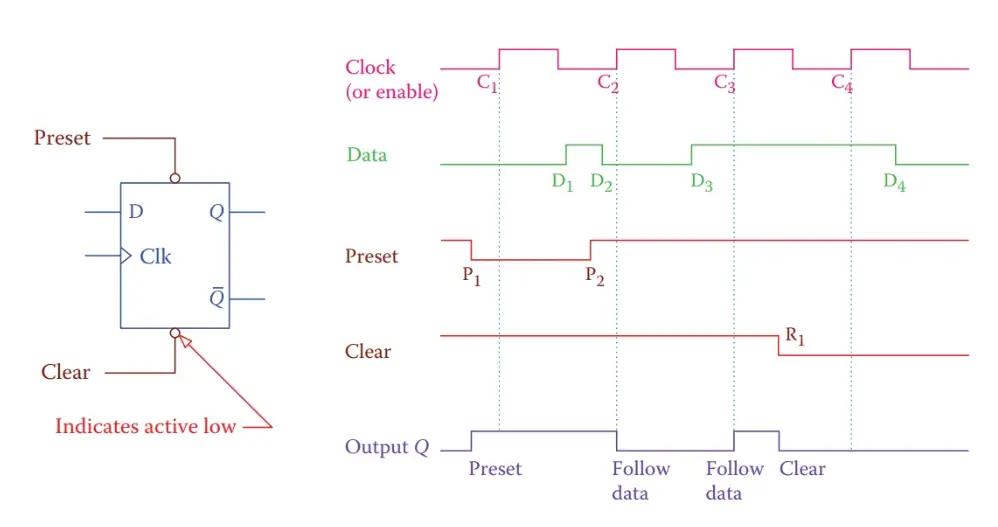
Figure 10 Flip-flop with preset and clear.