The bandpass and notch (or band-stop) filters are designed to pass or block a specified range of frequencies. As a review, the primary frequencies are identified on the frequency response curves in Figure 1. As you can see, each of these filters has two cutoff frequencies, designated fC1 and fC2. The difference between the cutoff frequencies is referred to as the bandwidth (BW) of the filter and the geometric average of the cutoff frequencies is referred to as its center frequency (f0).
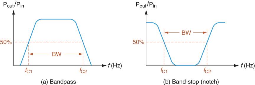
Figure 1: bandpass and band-stop filter frequency response
There are many possible approaches to building bandpass and notch filters. Most common bandpass ad notch filters are LC filters, like those shown in Figure 2. The circuits in Figure 2a are bandpass filters. The circuits in Figure 2b are notch filters. In each case, the filtering action is based on the resonant characteristics of the LC circuits.
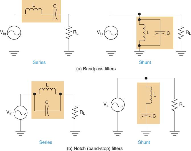
Figure 2: LC bandpass and band-stop filters Circuits
The basic characteristics of series and parallel resonant circuits are listed in Figure 3.
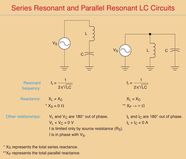
Figure 3: characteristics of series and parallel resonant circuits
Series LC Band Pass Filter
The operation of a series LC bandpass filter is easiest to understand when the filter represented as an equivalent circuit like the one in Figure 4b.
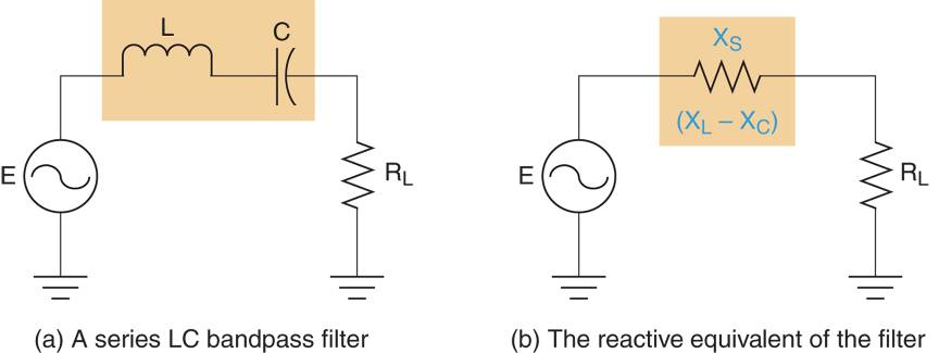
Figure 4: Series LC Bandpass Filter Circuit
In this circuit, the net series reactance (XS) of the filer is represented as a series component between the source and the load.
The operation of a series LC bandpass filter is based on the relationship between its input frequency and resonant frequency, as follows:
• fin = fr When the circuit is operating at resonance, the component reactances are equal and XS = XL – XC = 0Ω. This means that ignoring RW, the circuit current is determined by the source voltage and the load (IT = E/RL). The circuit resistive in nature and the phase angle is 0o.
• f in < fr. When the input frequency drops below fr, XC increases and XL decreases. As a result, the net reactance is capacitive in nature and the impedance phase angle is negative. As fin continues to decrease XS increases in magnitude and the impedance phase angle becomes more negative. When fin reaches 0Hz, XC and XS approach infinity and IT = 0A.
• fin > fr. When the input frequency rises above fr, Xc decreases and XL increases. As a result, the net reactance is inductive in nature and the impedance phase angle is positive. As fin continues to increase, XS increases in magnitude and the impedance phase angle becomes more positive. When fin approaches infinity, XL and XS approach infinity and IT = 0A.
The curve in Figure 5 illustrates the frequency of response of a series LC bandpass filter.
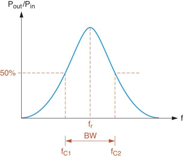
Figure 5: Frequency Response Curve of an LC Bandpass Filter
Shunt LC Band Pass Filters
Once you understand the operation of the series LC band pass filter, the operation of its shunt counterpart is relatively easy to visualize. A shunt LC bandpass filter is shown in Figure 6, along with its reactive equivalent circuit. Note that XP and XC, as indicated by the equation.
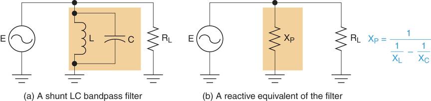
Figure 6: Shunt LC Bandpass Filter Circuit
Here is how the parallel LC circuit responds to frequencies above, below, and at resonance.
• fin = fr. When the circuit is operating at resonance, IL = IC and XP approaches infinity. As a result, the filter is effectively removed from the circuit and VRL ≡ E. In this case, the circuit is resistive in nature and the phase angle is 0o.
• fin < fr. When the input frequency drops below fr, XL decreases. As fin approaches 0Hz, the reactance of the shunt inductor approaches 0Ω, which shorts out the load. In this case, VRL ≡ 0V.
• fin > fr. When the input frequency rises above fr, XC decreases. As fin continues to increase, XC approaches 0Ω, which shorts out the load. Again, VRL = 0V.
Note that the frequency response curve for the circuit in Figure 5 is nearly identical to the one shown in Figure 4. Even though the two circuits operate differently, they produce the same overall frequency response.
Filter Quality (Q)
The Q of an inductor is a measure of how close the component comes to the ideal inductor, found as:
\[Q=\frac{{{X}_{L}}}{{{R}_{W}}}\]
Where RW = the winding resistance of the coil.
The ideal inductor would have a winding resistance (RW) of 0Ω. As a result, the total opposition to current (Z) presented by the inductor would equal XL. Note that the higher the Q of the component, the closer it comes to the ideal of Z=XL.
It should be noted that the addition of a resistive load o a series or parallel LC filter reduces the Q of the circuit. We will address the effects of loading on filter Q later in this section.
Series Filter Frequency Analysis
In section 1, you were shown how to calculate the bandwidth of a bandpass filter when the center frequency (f0) and filter quality (Q) are known. The relationship between these filter characteristics is given as:
$BW=\frac{{{f}_{0}}}{Q}$
The center frequency of an LC bandpass filter equals the resonant frequency of the circuit. Therefore, the bandwidth of a series LC bandpass filter can be found as:
\[\begin{matrix}BW=\frac{{{f}_{r}}}{{{Q}_{L}}} & {} & \left( 1 \right) \\\end{matrix}\]
The loaded-Q (QL) of a filter is the quality (Q) of the circuit when a load is connected to its output terminals. The concept of Q loading is illustrated in Figure 7. As stated earlier, the Q of an inductor equals the ratio of inductive reactance to winding resistance. More precisely, it is the ratio of XL to the total series resistance. As you can see, the total resistance of figure 6 equals the sum of the winding resistance and the load resistance. Therefore, the loaded Q of the circuit is found as:
\[\begin{matrix}{{Q}_{L}}=\frac{{{X}_{L}}}{{{R}_{S}}+{{R}_{W}}+{{R}_{L}}} & {} & \left( 2 \right) \\\end{matrix}\]
The calculation of QL for the circuit in Figure 7 is shown in the figure. As you can see, the loaded-Q is significantly lower than the value of Q we would have obtained using only the inductor winding resistance.
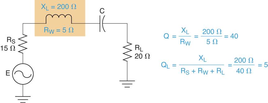
Figure 7: The values of Q and QL for an Inductor
To determine the bandwidth of a series LC bandpass filter, you must first calculate its resonant frequency. Then, you calculate the values of XL and QL at the resonant frequency. Finally, the values of fr and QL are used to determine the circuit bandwidth. Example 1 demonstrates this series of circuit calculations.
Example 1
Determine the bandwidth of the series LC Bandpass filter in Figure 7a.
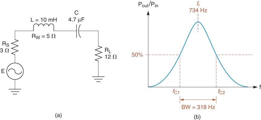
Figure 7a-b
Solution
First, the resonant frequency of the circuit is found as:
\[{{f}_{r}}=\frac{1}{2\pi \sqrt{LC}}=\frac{1}{2\pi \sqrt{10mH\times 4.7\mu F}}=734Hz\]
When the circuit is operated at this frequency, the value of XL is found as:
${{X}_{L}}=2\pi fL=2\pi \times 734Hz\times 10mH=46.1\Omega $
The circuit is shown to have the values of RS=3Ω, RW=3Ω, and RL=3Ω. Therefore, the loaded-Q of the component (at the resonant frequency) is found as:
\[{{Q}_{L}}=\frac{{{X}_{L}}}{{{R}_{S}}+{{R}_{W}}+{{R}_{L}}}=\frac{46.1\Omega }{20\Omega }=2.31\Omega \]
Finally, the bandwidth of the series bandpass filter can be found as:
\[BW=\frac{{{f}_{r}}}{{{Q}_{L}}}=\frac{734Hz}{2.31}=318Hz\]
The bandwidth and center frequency of the circuit are identified on the frequency response curve in Figure 7b.
Once we know the bandwidth and center frequency of a series bandpass filter, we have the information needed to calculate the circuit cutoff frequencies. When QL = 2, the center (resonant) frequency (fr) falls about halfway between the cutoff frequencies. As a result, the cutoff frequencies for a series bandpass filter can be found as:
\[\begin{matrix}{{f}_{C1}}={{f}_{r}}-\frac{BW}{2} & {} & \left( 3 \right) \\\end{matrix}\]
And
\[\begin{matrix}{{f}_{C2}}={{f}_{r}}+\frac{BW}{2} & {} & \left( 4 \right) \\\end{matrix}\]
Example 2 applies these relationships to the circuit we analyzed in Example 1.
Example 2
Determine the cutoff frequencies for the circuit in Figure 7a.
Solution
In example 1, the circuit was found to have the following values:
$\begin{matrix}{{Q}_{L}}=2.31 & {{f}_{r}}=734Hz & BW=318Hz \\\end{matrix}$
Since QL>2, we can calculate the values of the cutoff frequencies as:
${{f}_{C1}}={{f}_{r}}-\frac{BW}{2}=734Hz-\frac{318Hz}{2}=575Hz$
And
${{f}_{C2}}={{f}_{r}}+\frac{BW}{2}=734Hz+\frac{318Hz}{2}=893Hz$
When a filter has a value of QL < 2, the average frequency (fAVE) for the circuit must be calculated using:
\[\begin{matrix}{{f}_{AVE}}={{f}_{r}}\sqrt{1+{{\left( \frac{1}{2{{Q}_{L}}} \right)}^{2}}} & {} & \left( 5 \right) \\\end{matrix}\]
Once the value of fAVE is determined, then the cutoff frequencies can be calculated using:
$\begin{matrix}{{f}_{C1}}={{f}_{AVE}}-\frac{BW}{2} & {} & \left( 6 \right) \\\end{matrix}$
And
$\begin{matrix}{{f}_{C2}}={{f}_{AVE}}+\frac{BW}{2} & {} & \left( 7 \right) \\\end{matrix}$
These two equations are simply modified versions of the relationships we used in Example 2.
Shunt Filter Frequency Analysis
The analysis of a shunt LC bandpass filter is nearly identical to that of the series filter. The primary difference lies in the calculation of QL. For example, consider the circuit shown in Figure 8a. To determine the value of QL for this circuit, we need to combine RW with the other resistor values.
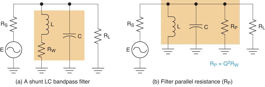
Figure 8: A Shunt LC Bandpass Filter and its equivalent Circuit
In the configuration shown, calculating the total circuit resistance is extremely difficult. However, the winding resistance of the coil can be represented as an equivalent parallel resistance (RP) as shown in Figure 8b. This parallel resistance, which represents the effective DC resistance of the filter, has a value that is found as:
$\begin{matrix}{{R}_{P}}={{Q}^{2}}{{R}_{W}} & {} & \left( 8 \right) \\\end{matrix}$
Where
Q= the unloaded Q of the filter
From the viewpoint of the filter, the three resistors in Figure 8b are in parallel. Using the parallel combination of the resistors the loaded Q of the circuit is found as:
\[\begin{matrix}{{Q}_{L}}=\frac{{{R}_{S}}||{{R}_{P}}||{{R}_{L}}}{{{X}_{L}}} & {} & \left( 9 \right) \\\end{matrix}\]
Example 3 demonstrates the process used to calculate the loaded Q of a shunt bandpass filter.
Example 3
Determine the value of QL for the circuit shown in Figure 8a.
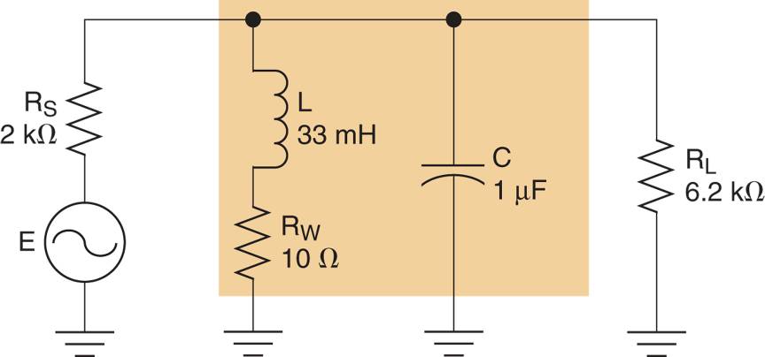
Figure 8a
Solution
First, the resonant frequency of the circuit is found as:
\[{{f}_{r}}=\frac{1}{2\pi \sqrt{LC}}=\frac{1}{2\pi \sqrt{33mH\times 1\mu F}}=876Hz\]
Now, the value of XL at the resonant frequency is found as:
${{X}_{L}}=2\pi fL=2\pi \times 876Hz\times 33mH=182\Omega $
The Q of the inductor is found as:
\[Q=\frac{{{X}_{L}}}{{{R}_{W}}}=\frac{182\Omega }{10\Omega }=1.82\]
Using the inductor Q, the value of RP is found as:
${{R}_{P}}={{Q}^{2}}{{R}_{W}}={{18.2}^{2}}\times 10\Omega =3.31k\Omega $
Finally, the loaded Q of the filter is found as:
\[{{Q}_{L}}=\frac{{{R}_{S}}||{{R}_{P}}||{{R}_{L}}}{{{X}_{L}}}=\frac{2k\Omega ||3.31k\Omega ||6.2k\Omega }{182\Omega }=5.7\]
Once the value of QL for a shunt bandpass filter has been determined, the rest of the frequency analysis proceeds just as it did for the series bandpass filter, as demonstrated in Example 4.
Example 4
Calculate the bandwidth and cutoff frequencies for the filter in Figure 8a.
Solution
From example 3, we know that the circuit has the following values:
$\begin{matrix}{{f}_{r}}=876Hz & {} & {{Q}_{L}}=5.7 \\\end{matrix}$
Using these values, the bandwidth of the filter can be found as:
\[BW=\frac{{{f}_{r}}}{{{Q}_{L}}}=\frac{876Hz}{5.7}=154Hz\]
Since QL>2, we can calculate the values of the cutoff frequencies as:
${{f}_{C1}}={{f}_{r}}-\frac{BW}{2}=876Hz-\frac{154Hz}{2}=799Hz$
And
${{f}_{C2}}={{f}_{r}}+\frac{BW}{2}=876Hz+\frac{154Hz}{2}=953Hz$
Using these values and those calculated in example 3, the frequency response curve for the circuit is plotted as shown in Figure 8b.
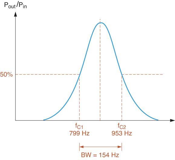
Figure 8b: Frequency Response Curve
There is an interesting point to be made: While the ideal parallel LC circuit has an infinite impedance at resonance, the impedance of the practical circuit is significantly lower. This impedance, which is resistive in nature, is represented by RP.
Series LC Notch Filters
A series LC notch filter can be constructed by placing a parallel LC circuit in series between the signal source and the load. Such a circuit is shown in Figure 9, along with its frequency response curve.
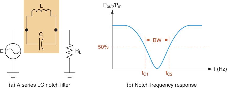
Figure 9: A Series LC Notch (band-stop) Filter Circuit and its frequency response curve
The operation of the series LC notch filter is easy to understand when you consider the circuit response to each of the following conditions:
$\begin{matrix}{{f}_{in}}=0Hz & {{f}_{in}}={{f}_{r}} & {{f}_{in}}=\infty Hz \\\end{matrix}$
- When fin = 0Hz, the reactance of the filter inductor is 0Ω. In this case, the signal source is coupled directly to the load via the inductor, and VRL = E. We say these values are approximately equal because some voltage is dropped across the winding resistance (RW) of the coil. However, the value of RW is typically much lower than the load resistance, so the approximation is valid in most cases.
- When fin = fr, the impedance of the LC filter is infinite for all practical purposes. In this case, the LC circuit isolates the source from the load, and VRL = 0V, The increase in the impedance of the LC circuit as frequency increases from 0 Hz to the value of fr accounts for the drop of load voltage. As the impedance of the LC filter increases, the filter drops more and more of the AC input signal. The resulting decrease in load voltage accounts for the slope of the frequency response curve as it foes from 0Hz to fr.
- As fin approaches ∞ Hz (a theoretical value), the reactance of the filter capacitor approaches 0Ω. In this case, the signal source is coupled directly to the load via the capacitor, Again, VRL = E.
Shunt LC Notch Filter
A shunt LC notch filter can be constructed by placing a series LC circuit in parallel with a load. Such a circuit is shown in Figure 10. The frequency response curve of the circuit is identical, for all practical purposes, to the one shown in Figure 9b.
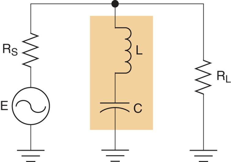
Figure 10: A Shunt LC Notch (Band-Stop) Filter Circuit
The operation of the shunt LC notch filter is easy to understand when you consider the circuit response to each of the following conditions:
$\begin{matrix}{{f}_{in}}=0Hz & {{f}_{in}}={{f}_{r}} & {{f}_{in}}=\infty Hz \\\end{matrix}$
- When fin = 0 Hz, the reactance of the capacitor is infinite, so the LC circuit acts as an open. As a result, the circuit effectively consists of the signal source, RS, and the load. In this case, VRL = E – VRS.
- When fin = fr, the LC circuit essentially shorts out the load. In this case, the load voltage is approximately 0V. The impedance of the LC circuit decreases from ∞Ω to 0Ω as the input frequency increases from 0 Hz to fr. This decrease in impedance causes the voltage across the LC circuit to decrease. Since the LC circuit in parallel with the load, load voltage also decreases. This accounts for the decrease shown in the frequency response curve (Figure 9b).
- When fin approaches ∞ Hz (a theoretical value), the reactance of the filter inductor is infinite. Therefore, the LC circuit acts as an open, just as it did when fin = 0Hz. The increase in filter impedance as frequency increases from fr to ∞ Hz causes the voltage across the filter to increase. Since the load is in parallel with the LC filter, load voltage also increases. This accounts for the rise shown in the frequency response curve (Figure 9b).