This article provides a brief introduction to PN junction diodes and BJT transistors.
Doping Silicon: N-Type and P-Type Semiconductors
PN junctions play an important role in semiconductor fabrication for integrated circuits. An undoped silicon with a valence of four has an intrinsic concentration of ${{n}_{i}}=1.1\times {{10}^{16}}\text{ }carriers/{{m}^{3}}$ at room temperature. This basically means that there are approximately $1.1\times {{10}^{16}}$ carriers of free electrons and holes per cm3in the pure silicon.
If we doped the silicon with an impurity that has a valence of five (equivalently five electrons in the outer shell) such as phosphorus (P) or arsenic (As), we are putting extra free electrons into the silicon crystal. Such impurity is therefore known as a donor and the doped region is called n-type region. In this n-type region, the number of free electrons nn is approximately equal to the impurity doping concentration ND and the number of holes is given by:
\[{{p}_{n}}=\frac{n_{i}^{2}}{{{N}_{D}}}\]
Forming PN Junction Diodes
To form a PN junction diode, one part of a semiconductor is doped as an n-type region and on top of it, another part is doped as a p-type region. A typical cross-section of a PN diode is as below:

The PN junction diode is formed between the p+ region and n region junction, where p+, p- and n represents different impurity doping concentration. As the PN junction was formed, a depletion region where no free carriers exist lies at the junction and the built-in voltage of an open-circuit PN junction is:
\[{{\Phi }_{0}}={{V}_{T}}ln\frac{{{N}_{A}}{{N}_{D}}}{n_{i}^{2}}\]
Where ${{V}_{T}}=\frac{kT}{q}\approx 26mV$ at room temperature, T is the temperature in degrees Kelvin, k is Boltzmann’s constant (1.38×10⁻²³JK) and q is the charge of an electron (1.6×10⁻¹⁹ Coulomb).
Positive Bias Voltage
If we apply a positive bias voltage from the p side to the n side of the PN junction diode, it reduces the electric field opposing the diffusion of the free carriers across the depletion region, as well as the depletion region width. If the applied positive voltage is large enough, the carriers will diffuse across the junction and therefore a current from the p side to the n side is formed. This positive voltage is called forward-bias voltage and is approximately 0.5V for silicon.
In this forward-bias region, the diode current-voltage relationship is given as below:
\[{{I}_{D}}={{I}_{S}}{{e}^{{}^{{{V}_{D}}}/{}_{{{V}_{T}}}}}\]
Where VD is the voltage applied across the diode and IS is the scaled current proportional to the area of the diode junction and inversely proportional to the doping concentrations. The exponential relationship comes from solving the first-order differential equation according to Fick’s law of diffusion.
Negative Bias Voltage
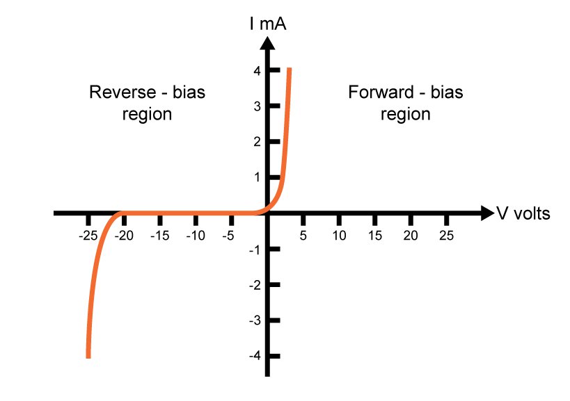
On the other hand, if we apply a negative bias voltage from the p side to the n side, i.e. a positive bias voltage from the n side to the p side, the PN junction diode is in reverse-biased region and has a small leakage current flow due to the minority carriers (holes and electrons) in the vicinity of the depletion region. However, at a critical electric field, the carriers traversing the depletion region acquire sufficient energy to create new hole-electron pairs in collisions with silicon atoms, causing avalanche breakdown and a sudden increase in the reverse-bias leakage current (the newly created carriers are also producing more new carriers).
A typical I-V characteristic for a junction diode is shown below:
Bipolar Junction Transistor
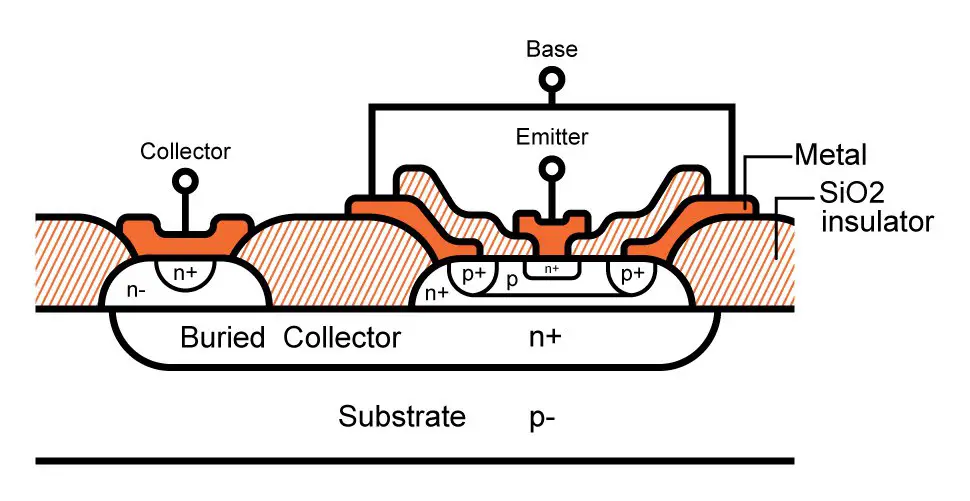
Similarly, a bipolar-junction transistor is made up of two PN junctions (either PNP or NPN) as below, taking NPN bipolar junction transistor as an example:
If the base-emitter voltage is less than the PN junction forward-bias voltage which is about 0.5V, the transistor will be cut off and no current flows from emitter to collector.
When the base-emitter voltage is large enough to turn on the PN junction, a small current will flow from the base to the emitter.
However, a much larger proportional current will flow from the collector to the emitter since the base width is rather small. Therefore, a bipolar transistor is a current amplifier since we can control the current from the collector to the emitter by adjusting the current from the base to the emitter.
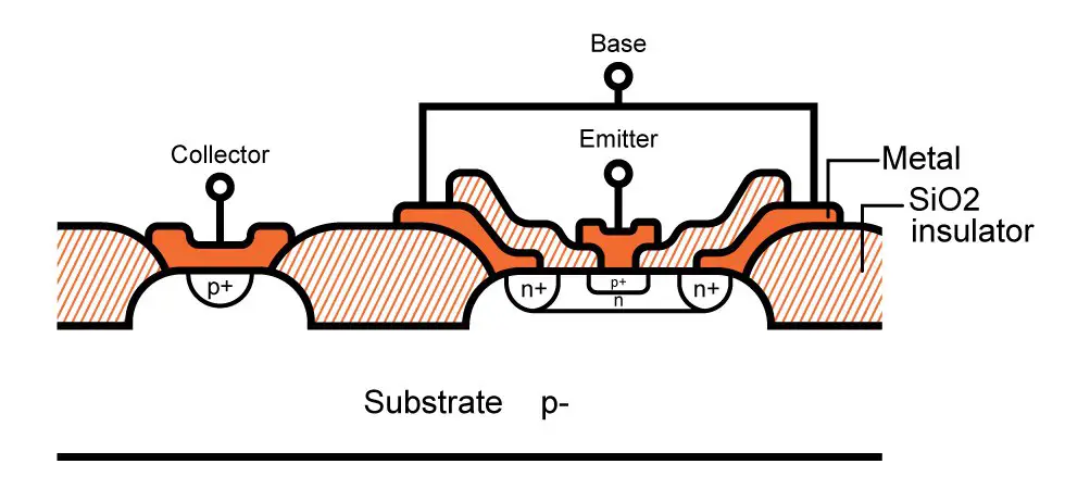
Correspondingly, a PNP transistor is shown below:
A PNP transistor behaves like an NPN transistor in reverse.
If the emitter-base voltage is less than the PN junction forward-bias voltage which is about 0.5V, the transistor will be cut off and no current flows from emitter to collector.
When the emitter-base voltage is large enough to turn on the PN junction, a small current will flow from the emitter to the base. It is clear that the required VBE to turn on an NPN transistor is about 0.5V, and the required VBE to turn on a PNP transistor is about -0.5V.
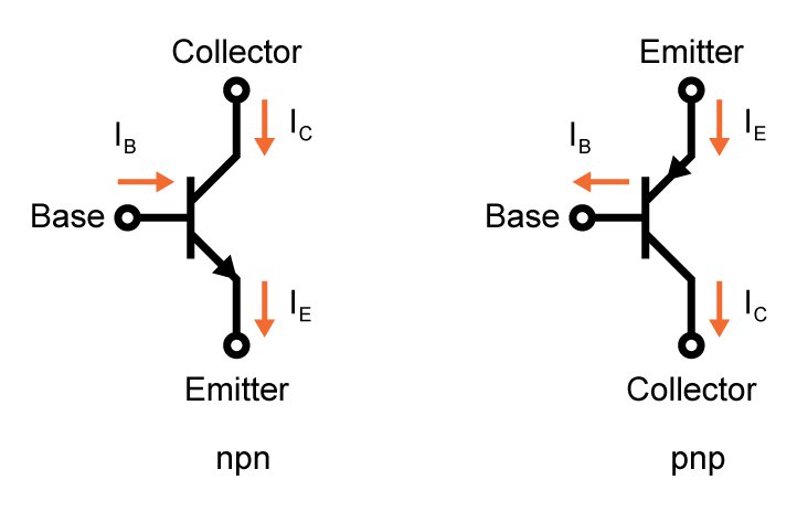
The symbols that represent NPN and PNP bipolar transistors are shown below:
The following equation describes the exponential relationship between the collector current and the base-emitter voltage:
${{I}_{C}}={{I}_{CS}}{{e}^{{}^{{{V}_{BE}}}/{}_{{{V}_{T}}}}}$
Where ICS is the scale current of the bipolar-junction transistor. The base current is also exponentially related to the base-emitter voltage as below:
\[{{I}_{B}}={{I}_{CS}}{{e}^{{}^{{{V}_{BE}}}/{}_{{{V}_{T}}}}}\]
Therefore the ratio of the base current and the collector current is a fixed ratio β as below:
\[\beta \equiv \frac{{{I}_{C}}}{{{I}_{B}}}\]
With the above equations, a large-signal model for a BJT in an active region can be drawn as follows:
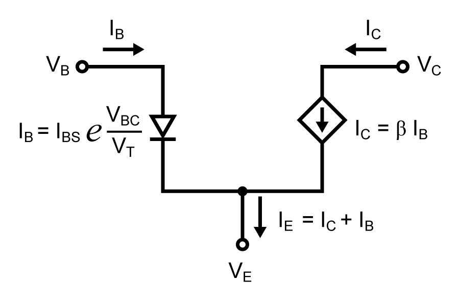
We have:
\[{{I}_{E}}={{I}_{C}}+{{I}_{B}}={{I}_{CS}}\left( \frac{\beta +1}{\beta } \right){{e}^{{}^{{{V}_{BE}}}/{}_{{{V}_{T}}}}}\equiv {{I}_{ES}}{{e}^{{}^{{{V}_{BE}}}/{}_{{{V}_{T}}}}}\]
We also often define
\[{{I}_{C}}=\alpha {{I}_{E}}\]
Where
\[\alpha =\frac{\beta +1}{\beta }\]
References
Analog Integrated Circuit Design, 2nd Edition, Tony Chan Carusone, David A. Johns and Kenneth W. Martin
Analysis and Design of Analog Integrated Circuits, 4th Edition, Paul R. Gray, Paul J. Hurst, Stephen H. Lewis and Robert G. Meyer
Design of Analog CMOS Integrated Circuits, 1st Edition, Behzad Razavi