The article provides an overview of the main types of photovoltaic (PV) cells, including monocrystalline, polycrystalline, and thin-film solar panels, and discusses their structures, efficiencies, and costs. It also introduces emerging PV technologies like dye-sensitized and organic photovoltaic cells, highlighting ongoing advancements in solar energy.
The three main types of photovoltaic (PV) cell include two types of crystalline semiconductors (Monocrystalline, Polycrystalline) and amorphous silicon thin film. These three types account for the most market share.
Two other types of PV cells that do not rely on the PN junction are dye-sensitized solar cells and organic photovoltaic cell.
PV technology is a rapidly growing field and many improvements, especially in efficiency and cost, can be expected.
Basic Types of Photovoltaic (PV) Cell
Photovoltaic cells are made from a variety of semiconductor materials that vary in performance and cost. Basically, there are three main categories of conventional solar cells: monocrystalline semiconductor, the polycrystalline semiconductor, an amorphous silicon thin-film semiconductor.
Monocrystalline Solar Panel
The crystallinity of a material indicates how perfectly ordered the atoms are in the crystal structure. The atoms making up a crystal are repeated in a regular, orderly manner.
The uniformity of the molecular structure of monocrystalline semiconductor (single-crystal) is ideal for electrons to move efficiently through the material.
An example of a monocrystalline semiconductor is monocrystalline silicon. This is the most widely used type of silicon in wafer-type solar cells because it has the highest efficiency. The drawback is that it is also the most expensive.
Typically, the efficiency of monocrystalline Si cells ranges from 14% to 18%, although occasionally you will see 19% to 20% specified.
Another monocrystalline semiconductor is gallium arsenide (GaAs), which is a compound. It is a better absorber of photons than silicon is and generally exhibits higher efficiency. One disadvantage of GaAs is that it is more expensive than silicon to use in PV cells.
Its main application is in concentrating PV applications, where a much smaller amount of material is required in a cell. GaAs cells are also commonly used in satellites and other space applications because of their high resistance to heat.
Polycrystalline Solar Panel
This type of semiconductor cell generally has a lower conversion efficiency compared to monocrystalline cells, but manufacturing costs are also lower.
The polycrystalline material is composed of numerous smaller crystals so that the orderly arrangement is disrupted from one crystal to another.
A common example of a polycrystalline cell is polycrystalline silicon. Cell efficiency typically is 13% to 15%. Polycrystalline silicon is also widely used because it is less expensive than monocrystalline silicon.
A variation on the polycrystalline silicon wafer is ribbon silicon, which is formed by drawing flat thin films from molten silicon. Although less efficient, ribbon silicon cells are less costly because their production does not require sawing wafers from ingots.
Another polycrystalline cell is cadmium-telluride (CdTe) thin-film. It uses the compound CdTe, which is a semiconductor with a band gap of 1.44 eV. This is a good match to the solar spectrum because it utilizes the portion of the solar spectrum with the highest energies. It also has high photon absorption. It is less expensive than silicon and has a higher efficiency than amorphous silicon.
Figure 1 shows the structure of a basic CdTe photovoltaic cell. The cadmium sulfide (CdS) layer is doped as an n-type material, and the thicker CdTe layer is doped as p-type and is the main energy absorber.
In some variations, the CdTe layer is intrinsic (not doped) and another layer of p-doped material, such as zinc telluride (ZnTe), is added below to create an electric field through the CdTe layer from the CdS layer to the ZnTe layer. This is done because p-type CdTe exhibits significant resistance, whereas intrinsic CdTe does not.
Another example of a polycrystalline semiconductor is copper-indium-gallium-diselenide (CuInGaSe2 CIGS]). This compound semiconductor material is commonly used in thin-film solar panels. It typically has higher efficiency than CdTe, and it has one of the highest absorption ratings of all semiconductors.
It can also produce more current per unit area than other thin-film technologies. Figure 2 illustrates the basic structure, although several variations are common.
Thin-Film Solar Panel
This type of solar panel is noncrystalline and can absorb up to forty times more solar radiation than monocrystalline silicon.
Thin-film photovoltaic solar panel uses layers of semiconductor materials from less than a micrometer (micron) to a few micrometers thick; wafer-type silicon cells can have thicknesses from 100 to several hundred micrometers.
Thin-films use much thinner semiconductor layers than wafer-type photovoltaic cells (typically hundreds of times thinner).
The advantage of thin-film solar panels is that they are much cheaper than crystalline solar panel because they use only a fraction of the material and because the manufacturing process is simpler.
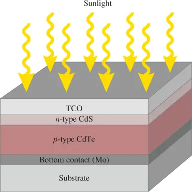
Figure 1: Structure of a Basic CdTe Thin-Film Photovoltaic
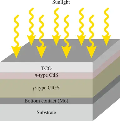
Figure 2: Structure of a Basic CIGS Thin-Film Photovoltaic Cell
Amorphous silicon (a-Si) has a higher band-gap energy (1.75 eV) than crystalline silicon (1.12 eV), which means it absorbs the visible part of the solar spectrum better than the infrared portion.
Thin-film a-Si solar cells are commonly known as hydrogenated amorphous silicon or a-Si: H. Amorphous silicon is deposited on low-cost fixed or flexible substrates such as plastics, glass, or other substrates using chemical vapor deposition or other methods.
Although amorphous silicon is the least expensive type of silicon photovoltaic material, its conversion efficiency is also the lowest. Typical conversion efficiencies range from 5% to 7% in spite of the higher light absorption.
Amorphous silicon, in its pure form, has defects in its atomic bonding that reduce its effectiveness in photovoltaic applications. It is usually alloyed with hydrogen to form a hydrogenated amorphous silicon (a-Si: H), which results in significantly fewer defects.
Figure 3 shows the cross-section of a hydrogenated amorphous silicon (a-Si: H) thin-film solar panel structure. A typical thin-film device doesn’t have a metal grid on the top electrical contact like a wafer-type silicon cell does.
Instead, it uses a thin layer of a transparent conducting oxide (TCO), such as the tin oxide that allows light to pass to the active layers below. These oxides are excellent conductors of electricity and serve as an electrode for the cell.
A p-i-n structure is usually used for generating and moving the electric charge in which an intrinsic layer (i) separates p and n regions. The intrinsic silicon layer (i-type a-Si: H) absorbs most of the photon energy and produces most of the electron-hole pairs.
The much thinner n-type and p-type layers primarily generate the electric field. The free electrons are swept toward the n-type layer, and the holes are swept toward the p-type layer by the electric field.
Some thin-films use a TCO and a reflective layer in place of the bottom contact of molybdenum (Mo) to increase the usable light energy by reflecting it back into the semiconductor layers. A glass protective layer is usually added on the top, as is a layer of anti-reflective material.
Other Types of Photovoltaic (PV) Cell
The PV materials previously discussed are all in production, with ongoing research to improve efficiency and lower the cost. Two other types of PV cells are newer and still largely in the research and development stage, but they are beginning to be commercialized for limited applications.
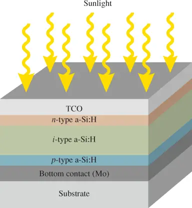
Figure 3: Structure of a Typical a-Si: H Thin-Film Photovoltaic Cell
Dye-Sensitized Solar Cell Working Principle
The dye-sensitized solar cell (DSSC) is a thin film cell that uses a process that is similar to the one plant’s use as they absorb sunlight in a dye (chlorophyll) and convert it to chemical energy. In the DSSC, however, the energy is ideally converted to electrical energy.
In its simplest form, the DSSC consists of a photo anode, a cathode, and a liquid electrolyte (or mediator solution). The photocathode consists of a thin layer of titanium dioxide (TiO2) that has been sensitized by a dye and deposited on a glass substrate.
When a photon is absorbed in the sensitized layer, an electron is moved to a higher energy level and is injected very rapidly into the conduction band of the TiO2 semiconductor. (A relatively few electrons recombine within the TiO2, without providing useful energy to the load.)
After passing through the external load, the electrons are passed back to the cell at the cathode, which is composed of an extremely thin (transparent) layer of platinum (Pt) deposited on a glass substrate.
Charge balance in the cell is maintained by moving the electrons collected at the cathode back to the dye layer through an electrolyte in a complex oxidation-reduction chemical reaction.
Dye cells have important advantages that offer possibilities for future applications.
For one thing, they do not require the expensive high-temperature and high-vacuum fabrication techniques that is required for silicon cells, so they can be fabricated readily without the expense of silicon cells.
- The TiO2a common pigment in the paint is plentiful, inexpensive, and nontoxic.
- Dye cells work in extremely low light conditions, which may be important in northern climates or indoor applications.
- Because dye cells can be manufactured at low cost, the payback period (the time required for the cell to produce as much energy as it took to manufacture it) may become better as the technology improves.
A disadvantage of dye cells is that they are much less efficient than solid-state cells and they require a liquid electrolyte. Much research is focused on increasing the efficiency and decreasing the cost of these cells by investigating alternatives to the anode, dyes, cathode, and electrolytes of dye cells.
Organic Photovoltaic (PV) Cell
Another type of thin-film cell is the organic photovoltaic cell (OPV). In its basic form, the OPV consists of a single layer of active polymer material (the dye) sandwiched between two electrodes.
Organic cells are flexible and are very low cost. They can be manufactured in large volume. One drawback is that they are inefficient. Researchers are currently working on improving these cells by using different materials, graded junctions, and production methods.
Photovoltaic (PV) Cell Review Questions
- What are three categories of materials used in silicon PV cells?
- What is a TCO layer and what does it do?
- What is the advantage of thin-film PV cells over wafer-type cells?
- What is the purpose of the dye in a DSSC?
Answers
- Monocrystalline semiconductor; polycrystalline semiconductor; and amorphous silicon, thin-film semiconductor.
- A TCO is a transparent conducting oxide. It conducts electric charge and serves as an electrode for the cell.
- Less costly to produce and the manufacturing process is simpler.
- The dye sensitizes the photocathode.
Photovoltaic (PV) Cell Key Takeaways
Understanding the various types of photovoltaic (PV) cells—monocrystalline, polycrystalline, and thin-film—as well as emerging technologies like dye-sensitized and organic PV cells, is essential for advancing solar energy applications. Each type offers a unique combination of efficiency, cost, and adaptability that makes it suitable for specific environments and use cases. For example, high-efficiency monocrystalline cells are ideal for space-constrained rooftops, while low-cost thin-film and emerging dye-sensitized or organic cells open up possibilities for flexible, portable, and indoor applications.