In this article, the PN junction, which forms the basis of photovoltaic devices, is introduced. Silicon (Si) is the most common element used in the construction of photovoltaic solar cells.
Recall that the addition of impurities to pure silicon (or other semiconductors) can change the conduction properties and form p and n materials depending on the specific impurity.
If part of a small block of silicon is doped with an n-type impurity and the other part with a p-type impurity, the boundary created between them is called a PN junction. The PN junction is essential to the operation of solar cells and many other semiconductor devices.
Silicon Atom and Crystal Structure
Silicon is one of the most abundant elements on earth and is found in sand and quartz as well as other natural sources. Silicon can form a crystalline structure (designated c-Si), or it can form an amorphous type of silicon that has a random arrangement of atoms (designated a-Si).
Both types are useful in solar cells. In this section, we will focus on c-Si and its use.
In c-Si, there is an orderly arrangement of covalently bonded silicon atoms. According to the Bohr model, an atom consists of a nucleus of protons and neutrons surrounded by orbiting electrons at various distances from the nucleus called shells.
- You May Also Read: PN Junction Diodes and BJT Transistors: an Introduction
The neutral silicon atom has 14 protons, 14 to 16 neutrons, and 14 electrons. The electrons in the outer shell of an atom are known as valence electrons, as shown in the atomic model for silicon in Figure 1(a). This outer shell of a semiconductor or insulator is known as the valence band and includes electrons that are bound to the atom. The valence electrons participate in bonding to other atoms.
In a silicon crystal, each silicon atom shares an electron with its four neighboring atoms, creating a four covalent bond as shown in Figure 1(b). Each atom in the crystal is bonded to its neighbors. Figure 1(c) illustrates the structure of a silicon crystal that has multiple atoms held together by the covalent bonds.
Doping a Silicon Crystal
As mentioned, silicon in its pure (intrinsic) state is a poor electrical conductor. The process of doping is used to increase the conductivity in a precise and controlled way.
The doping process adds impurity atoms in very low concentrations to the silicon to create an excess of free electrons (n-type impurity). The place where a deficiency occurs is called a hole.
Pentavalent Impurity
A pentavalent impurity atom has five valence electrons and, when added to a silicon crystal, four of its electrons form covalent bonds with four adjacent silicon atoms. One electron is left and becomes an unbonded or free electron, as illustrated in Figure 2(a). Examples of pentavalent atoms are phosphorous (P), arsenic (As), antimony (Sb), and bismuth (Bi).
Trivalent Impurity
A trivalent impurity atom has three valence electrons and, when added to a silicon crystal, three of its electrons form covalent bonds with four adjacent silicon atoms. An electron vacancy or hole is created in one of the bonds, as illustrated in Figure 2(b). Examples of trivalent atoms are boron (B), indium (In), and gallium (Ga).
Formation of the PN Junction
Figure 3(a) shows the formation of the PN junction between n-type and p-type regions of a piece of silicon that has been doped with phosphorous in the top part and with boron in the bottom part. The free electrons in the n region are randomly drifting in all directions.

Figure 1: Silicon Atom and Covalent Bonding Forms a Crystal Structure
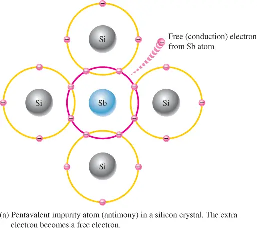
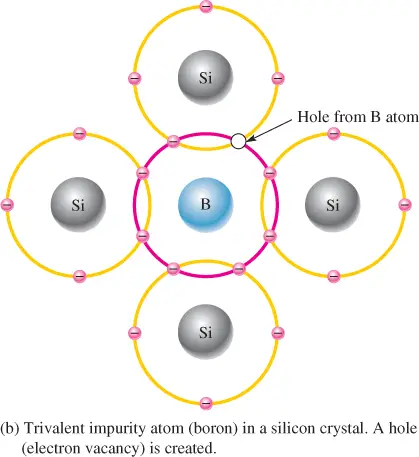
Figure 2: Doping a Silicon Crystal
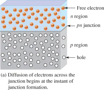

Figure 3: PN Junction and Depletion Region
At the instant of PN junction formation, the free electrons near the junction in the n region begin to diffuse across the junction into the p region, where they combine with holes near the junction.
Before the PN junction is formed, there are as many electrons as protons in the n-type material, making the material neutral in terms of charge. The same is true for the p-type material.
When the PN junction is formed, the n region loses free electrons as they diffuse across the junction. This creates a layer of positive charges (pentavalent ions) near the top side of the junction. As the electrons move across the junction, the p region loses holes as the free electrons and holes combine. This action creates a layer of negative charges (trivalent ions) near the bottom side of the junction. These two layers of positive and negative charges form the depletion region, as shown in Figure 3(b). The depletion region is depleted of charge carriers (electrons and holes).
Formation of the Depletion Region
The depletion region is very thin compared to the p and n regions. Its width is exaggerated in Figure 3(b) for purposes of illustration.
After the initial surge of free electrons across the PN junction, the depletion region expands to a point where equilibrium is established and there is no further diffusion of electrons across the junction. This process occurs because, as electrons continue to diffuse across the junction, more and more positive and negative charges are created near the junction and the depletion region forms. A point is reached where the total negative charge in the depletion region repels any further diffusion of electrons into the p-region and the diffusion stops.
The depletion region has many positive charges and many negative charges on opposite sides of the PN junction. The force between the positive and the negative charges form an electric field, indicated by the blue arrows in Figure 3(b). The electric field acts as a barrier to the free electrons in the n region, and external energy must be applied to move these electrons across the depletion region.
In diodes and transistors, the external energy comes from a voltage source; in solar cells, the external energy comes from sunlight.
Review Questions
- Describe the Bohr model of an atom.
- How is the n region in silicon created?
- How is the p region in silicon created?
- What is a PN junction?
- In the absence of an applied voltage, what keeps the electrons from crossing the depletion region?
Answers
- The Bohr model is a planetary model of the atom, with electrons orbiting in discrete orbits about a central nucleus containing neutrons and protons.
- By doping pure silicon with a pentavalent substance such as phosphorous or arsenic
- By doping pure silicon with a trivalent substance such as are boron or indium
- A PN junction is the boundary created between an n-type and a p-type semiconductor.
- The electric field that forms due to the migration of charge across the boundary
PN Junction Key Takeaways
The PN junction is a foundational element in semiconductor technology, particularly in photovoltaic solar cells and other electronic devices like diodes and transistors. Its ability to create an electric field through the formation of a depletion region allows it to control the movement of charge carriers, which is essential for the conversion of light into electrical energy in solar cells and for switching and rectifying functions in electronic circuits.