This article covers the characteristic curves of Junction Field-Effect Transistors (JFETs), explaining how changes in gate voltage affect the drain current and how to develop and interpret a JFET characteristic curve.
The JFET is very different from other solid-state components. A small change in gate voltage, for example, causes a substantial change in drain current. The JFET is, therefore, classified as a voltage-sensitive device. By comparison, bipolar transistors are classified as current-sensitive devices. A JFET has a rather unusual set of characteristics compared with other solid-state devices.
A drain family of characteristic curves is shown in Figure 1. The horizontal part of the graph shows the voltage appearing across the source drain as $V_{DS}$. The vertical axis shows the drain current ($I_{D}$) in milliamperes. Individual curves of the graph show different values of gate voltage ($V_{GS}$). The cutoff voltage of this device is approximately 7 V. The control range of the gate is from 0 to 6 V.
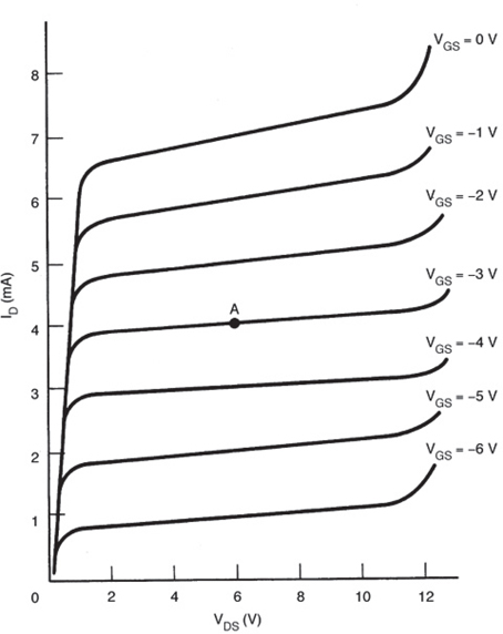
Figure 1. A drain family of characteristic curves for a JFET.
A drain family of characteristic curves tells a great deal about the operation of a JFET. For example, if a JFET has 3 V applied to its gate and a $V_{DS}$ of 6 V, approximately 4 mA of $I_{D}$ flows through the channel. This is determined by projecting a line to the left of the intersection of the 3 $V_{GS}$ and 6 $V_{DS}$. Any combination of $I_{D}$, $V_{GS}$, and $V_{DS}$ can be determined through the drain family of characteristic curves.
Example 1
If a JFET has 4 V applied to its gate and a $V_{DS}$ of 6 V, approximately how much drain current ($I_{D}$) would flow through the channel?
Solution
- Mark the intersection of $-4 V_{GS}$ and 6 $V_{DS}$.
- Project a line to the left of the intersection of -4 $V_{GS}$ and 6 $V_{DS}$. Approximately 3 mA of drain current would flow through the channel.
Developing a JFET Characteristic Curve
A special circuit is used to develop the data for a drain family of characteristic curves. Figure 2 shows a test circuit that is used to identify the different operating regions of an N-channel JFET. Drain current or $I_{D}$ is an indication of electron flow in the channel. The single characteristic curve of Figure 1 is the result of 0 $V_{GS}$. This curve shows how the drain current ($I_{D}$) is affected by drain-to-source voltage ($V_{DS}$) when the gate-to-source voltage is 0 $V_{GS}$. Gate voltage is monitored by a $V_{GS}$ meter connected between the gate-source leads. Drain current ($I_{D}$) is measured by a milliampere meter connected in series with the drain. $V_{DS}$ is measured with a voltmeter connected across the source and drain. $V_{GS}$ and $V_{DS}$ are adjusted to different values while $I_{D}$ is monitored. Two variable DC power supplies are used in the test circuit.
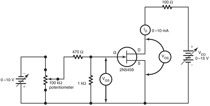
Figure 2. A drain family of characteristic curves test circuit for an N-channel JFET.
The data points of a single curve are developed by first adjusting $V_{GS}$ to 0 V. Normally, $V_{DS}$ is increased in 0.1-V steps up to 1 V. $I_{D}$ increases very quickly during this operational time. $V_{DS}$ is then increased in 1-V steps, while the $I_{D}$ values are recorded. Corresponding $I_{D}$ and $V_{GS}$ values are then plotted on a graph as the 0-$V_{GS}$ curve.
To develop the second curve, $V_{DS}$ must be returned to zero. $V_{GS}$ is then adjusted to a new value. A value of 1 $V_{GS}$ would be suitable for most JFETs. $V_{DS}$ is again adjusted through its range while $I_{D}$ is monitored. Data for the second curve is then recorded on the graph.
To obtain a complete drain family of characteristic curves, the process is repeated for several other $V_{GS}$ values. A typical family of curves may have 8-10 different values. The step values of $V_{DS}$, $V_{GS}$, and $I_{D}$ obviously change with different devices. Full conduction is usually determined first. This gives an approximation of representative $I_{D}$ and $V_{DS}$ values. Normally, $I_{D}$ levels off to a rather constant value when $V_{DS}$ is increased. $V_{DS}$ can be increased in value to a point where $I_{D}$ starts a slight increase. Generally, this indicates the beginning of the breakdown region. JFETs are usually destroyed if conduction occurs beyond this area of operation. Maximum $V_{DS}$ values for a specific device are available from the manufacturer. It is a good practice to avoid operation in or near the breakdown region of the device.
Review Questions
- A JFET is classified as a __________-sensitive device.
- The JFET characteristic curve shows how the drain current ($I_{D}$) is affected by the _________-to-source voltage ($V{DS}$).
- The horizontal axis in a JFET characteristic curve represents the __________ (VDS).
- The vertical axis in a JFET characteristic curve represents the __________ current ($I_{D}$).
- A JFET typically has a cutoff voltage of __________ V.
- The drain current ($I_{D}$) increases very quickly during the operational time when __________ is increased in steps of 0.1 V.
- The JFET test circuit measures the __________ current ($I_{D}$) with a milliampere meter.
- A typical drain family of characteristic curves may have __________ to __________ different values for $V_{GS}$.
- To develop a complete drain family of characteristic curves, the process must be repeated for several other __________ values.
- The breakdown region is typically avoided because JFETs are usually __________ if conduction occurs beyond this area.
Answers
- Voltage
- Drain
- Drain-to-source voltage
- Drain
- 7
- $V_{DS}$
- Drain
- 8, 10
- Gate-source voltage
- Destroyed
Key Takeaways
The JFET characteristic curves are essential for understanding the precise relationship between the gate voltage ($V_{GS}$), drain current ($I_{D}$), and drain-to-source voltage ($V_{DS}$). These curves allow engineers to determine the optimal operating conditions for JFETs, ensuring efficient performance in circuits.