The article provides an overview of integrated circuit (IC), covering their definition, historical development, and advantages over earlier technologies like transistors. It also explains the detailed construction process of ICs, including materials, design, fabrication, and testing stages.
Definition: An integrated circuit, or IC, is a complete electronic circuit contained in one package, Figure 1. This package often includes transistors, diodes, resistors, and capacitors along with the connecting wiring and terminals. An IC is also called a chip.
The transistor was invented in 1947 by Brattain, Bardeen, and Shockley of Bell Laboratories. The transistor served the same purpose as Lee DeForest’s triode amplifier, but it did not need heat to operate.
In addition, the transistor was solid (solid- state) and much smaller. Transistors were first used in small appliances such as hearing aids and small transistor radios. Small size and efficient operation also made transistors useful in defense items.
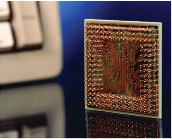
Figure 1. An integrated circuit (IC).
Transistors were also used in the newly developed electronic computer circuits of the 1950s and early 1960s.
Computers used thousands of switching circuits, and transistors were able to quickly perform this switching function. But as computer circuits became larger and more powerful, electronic circuits needed to become smaller.
Because the components of circuits have to be wired together, producing the smaller circuits was a complex task. Printed circuit boards helped, but the wiring was still bulky. This problem was solved by integrating all these components into one solid piece of material, the integrated circuit. See Figure 2.
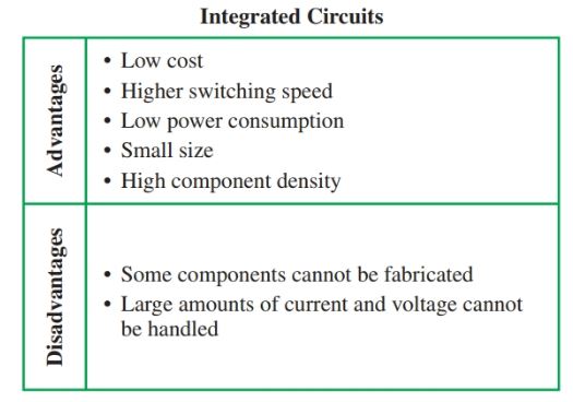
Figure 2. The advantages and disadvantages of ICs when compared with transistors.
History of the Integrated Circuit
In 1952, G.W.A. Dummer of the Royal Radar Establishment in Great Britain had the idea for an integrated circuit. However, his ideas were not put to use at that time.
In 1957, a new process for planar transistors was developed at Fairchild Semiconductors. This allowed semiconductor emitters, bases, and other parts to be made on the surface of a silicon wafer.
In early 1958, Jack Kilby of the Texas Instruments Corporation was developing micro-modules. These were to be made by printing the components on a ceramic wafer.
He realized that semiconductors and other components could be made on the same surface through a manufacturing process. The first commercially produced integrated circuit resulted from this work. It was made on a thin wafer of germanium. However, it still had wire connections, which caused a major problem when wiring together large numbers of transistors and other conductors.
About the same time, another process for making ICs was being studied at Fairchild Semiconductors. Using the principles of planar transistor manufacturing, Robert Noyce used silicon dioxide dopants to protect and insulate PN junctions.
The integrated circuit dramatically changed the electronics field. In 1965, about 30 components could be put on a silicon chip five millimeters (3/16 in.) square.
By 1982, that number had increased to 1,000,000, Figure 3. While the IC has become smaller and smaller, even reaching microscopic sizes, the principles of operation remain the same.
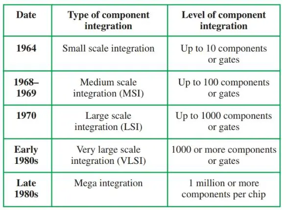
Figure 3. Levels of integration.
Integrated Circuit (IC) Construction
An integrated circuit consists of many extremely thin layers of P- and N-type material arranged in configurations such as transistors, diodes, resistors, and capacitors. A single chip may contain millions of transistors and occupy less than one square inch of area.
The circuit designer begins the production process by designing the complete integrated circuit. One factor affecting design is the intended use of the IC. With this in mind, the designer plans the best IC for use. He or she submits the completed design in the form of a schematic diagram.
From this schematic diagram, the layout designer creates a detailed technical drawing. The circuit is drawn in a much larger scale than the final product so that when the drawing is reduced there will be enough space between parts. Figure 4. If any of the lines touch each other, the circuit will short out when tested.
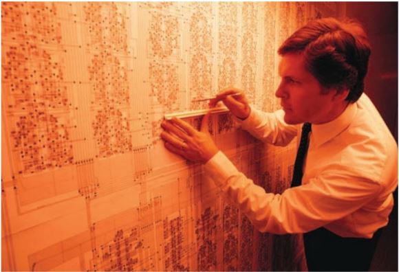
Figure 4. This circuit diagram will be reduced hundreds of times before it is used to make circuits.
Next, each circuit layout is photographically reduced. It is not unusual for the layout to be reduced over 1000 times or more. A reduced layout allows for thousands of circuits to be put on one wafer.
Working plates are made from the reduced layouts. These plates are called photomasks. Each photomask goes with a certain step in the production process. Each mask contains a large number of identical, actual size parts. The photomasks are now ready for use and production of the IC can now begin.
The structure of an IC is a pure silicon crystal. These pure crystals must first be produced. To make the crystal, liquid silicon is purified.
A solid silicon particle, or seed, is dipped into the melted silicon. It is slowly withdrawn and placed in a cool area, Figure 5.
The grown crystal is sliced into wafers about 0.5 mm thick. The wafers are then polished to rid the wafer of surface scratches and contaminants. Small portions of impurities are then added. The impurities give the silicon its electrical traits.

Figure 5. Pure silicon crystal. (Motorola)
On the thin wafers of doped silicon, the basic building process begins. The circuit is built layer by layer, on the silicon wafer, or substrate. Each layer receives a pattern from the photomask.
In the example shown in Figure 6, the first layer on top of the silicon is a layer of N-type material. It is grown right on the wafer, and it is called the epitaxial layer. Epitaxy is a growth of one crystal on the surface of another crystal. This is the collector for a transistor or an element of a diode.
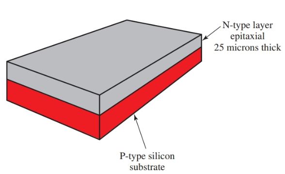
Figure 6. Growing N-type material on the P-type substrate.
Next, a thin coat of silicon dioxide is grown over the N-type material by exposing the wafer to an oxygen atmosphere at about 1000°C. See Figure 7.
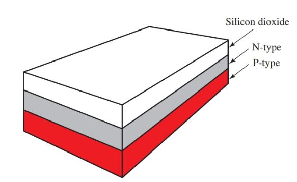
Figure 7. A silicon dioxide layer is placed on top of the N-type layer.
Next, a thin coat of a light-sensitive emulsion is placed over the N-type layer. The emulsion is called photoresist. In a process called photoengraving, the photomask is placed over the N-type layer. Then the entire wafer is exposed to ultraviolet light, Figure 8. The light causes the image of the photomask to transfer to the wafer.
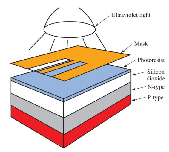
Figure 8. The photoengraving process
The exposed photoresist hardens. The areas covered by the mask remain soft. Acids or solvents are used to etch away the unexposed (soft) area of the photoresist. This leaves the layer of the N-type silicon exposed. Figure 9.
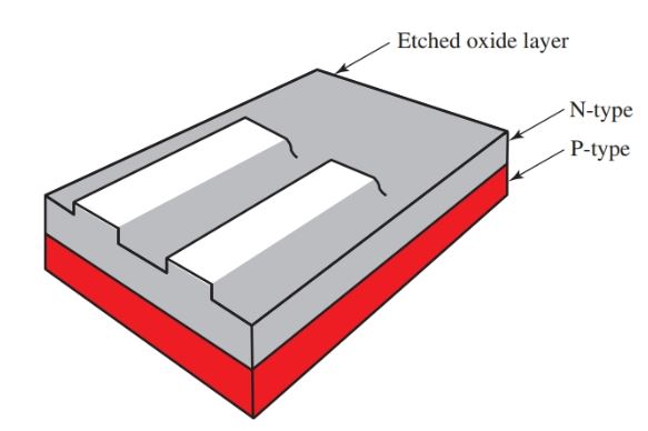
Figure 9. The first masking and etching isolate components.
The exposed N-type layer is further etched away by very hot gases. A chemical washes away any remaining hardened photoresist to expose all N-type silicon dioxide.
As parts of the IC are constructed, they must be isolated from each other. This is done by diffusion.
Diffusion is a process in which impurities are doped into the silicon wafer to form the needed junctions. Diffusion forms islands of N-type materials backing P-type materials.
The wafer is diffused using boron. The boron cuts into and forms a P-type material on all areas not protected by the silicon dioxide. The wafer has isolated islands of N-type material, Figure 10. NP junctions form around each island. There are back-to-back diodes between each N-type island.
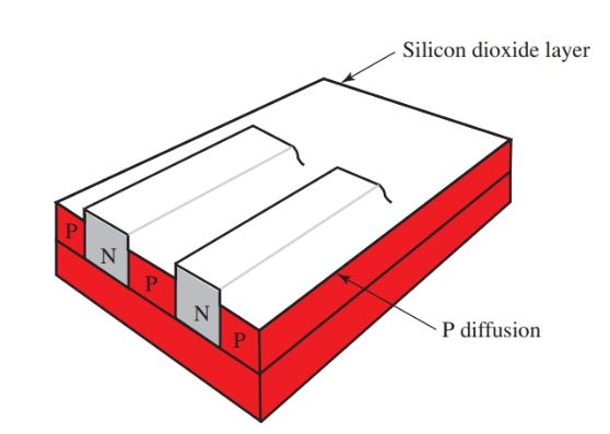
Figure 10. N-type material remains after P diffusion.
During diffusion, a new layer of silicon dioxide forms over the diffused P-type areas, as well as on top of the islands, Figure 11.
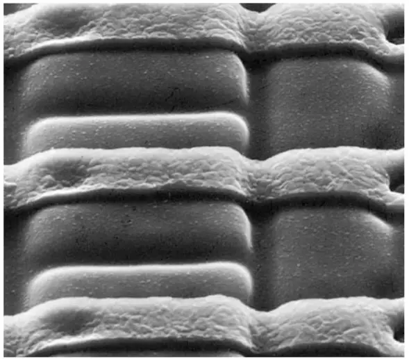
Figure 11. P-type diffusant on N-type silicon dioxide. (Lattice Semiconductor)
The wafer is again coated with photoresist and exposed under a photomask. Areas in the N-type islands are etched away. Once again, the wafer is subjected to a P-type diffusant that forms areas for transistor base regions, resistors, or elements of diodes or capacitors. The wafer is then re-oxidized Figure 12.
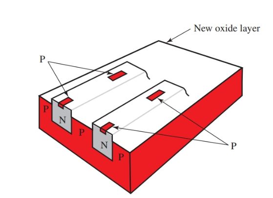
Figure 12. P-type regions are diffused in the N-type islands.
The wafer is again masked and exposed to open windows in the P-type regions. A phosphorus diffusant is used to produce N-type regions for diodes and capacitors.
Small windows are also etched through to the N layer for electrical connections, Figure 13. The total wafer is again given an oxide coating.
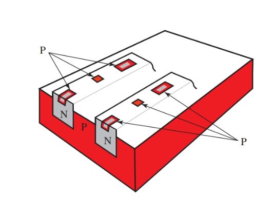
Figure 13. Windows are opened in the P-type regions.
The monolithic circuit is now complete except for the aluminum interconnections. The aluminum interconnections join the islands. They also join the circuit to other circuits and other devices.
A thin coat of aluminum is vacuum-deposited over the entire circuit. The aluminum coating is then sensitized and exposed through another special mask. After etching, only the interconnecting aluminum remains. It forms a pattern between transistors, diodes, and resistors, Figure 14.
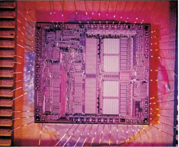
Figure 14. Aluminum interconnections. (Motorola)
The interconnections of an IC can be made from a metal or alloy. Currently, gold-plated leads are recommended for use only with socket-type IC devices.
Gold creates a brittle joint when used in a solder type connection. This results in a damaged connection when the board is subjected to excessive vibration or board flexing.
The completed circuits are then tested Figure 15. In a single test, the circuits are used to perform a series of electrical tasks, Figure 16.
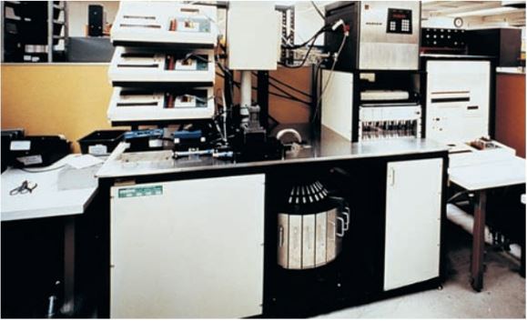
Figure 15. Wafer testing must take place in a sterile area. Even a small piece of dust can ruin a circuit. This machine automatically tests semiconductor parts for electrical specifications. (Motorola)
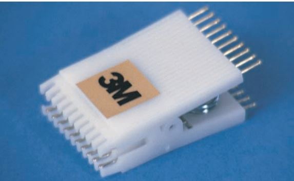
Figure 16. IC test clip.
After testing, the wafers are separated into individual chips, usually by scribing them with a diamond-tipped tool. The chips are then mounted onto a small can or flat package, Figure 17. Leads are bonded, and the ICs are washed. The cavities that hold the ICs are sealed, and finally, the ICs are shipped to a distributor.
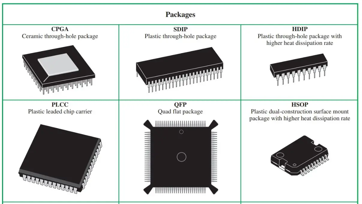
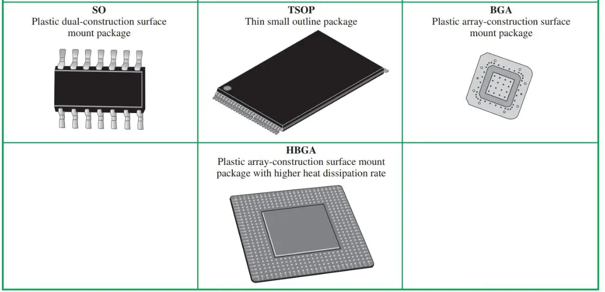
Figure 17. IC packages. (Motorola)
Resistors
The process just discussed is used to make semiconductor materials on ICs. This process can be used to make resistors, capacitors, and diodes.
Recall that N-type or P-type materials have certain resistances. Resistance depends on the physical size of the material (length or surface area) and the number of dopants in the material.
Semiconductors are made with very pure silicon. Through the doping process, impure trivalent or pentavalent atoms are added to produce the N-type or P-type substrate material.
For example, a P-type silicon material is used as the substrate. An N-type material is diffused into the surface of the chip, Figure 18. Then another P-type material is added to the N-type material. Metal leads are fastened to the end of this P-type material. The P-type material and its two connections are used as a resistor.
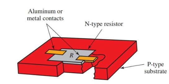
Figure 18. Resistors made on an integrated circuit
Capacitors
Like resistors, capacitors can be made in an integrated circuit. Values for these capacitors are very small. However, they are still able to perform functions of coupling and storage. Figure 19 shows how a capacitor can be made in an integrated circuit.
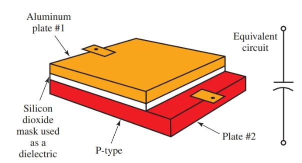
Figure 19. Capacitors made in an IC.
Putting It Together
An example of how a transistor, resistor, and capacitor can be integrated into one circuit is shown in Figure 20. Keep in mind that thousands of these circuits can be placed onto an area the size of the head of a pin.
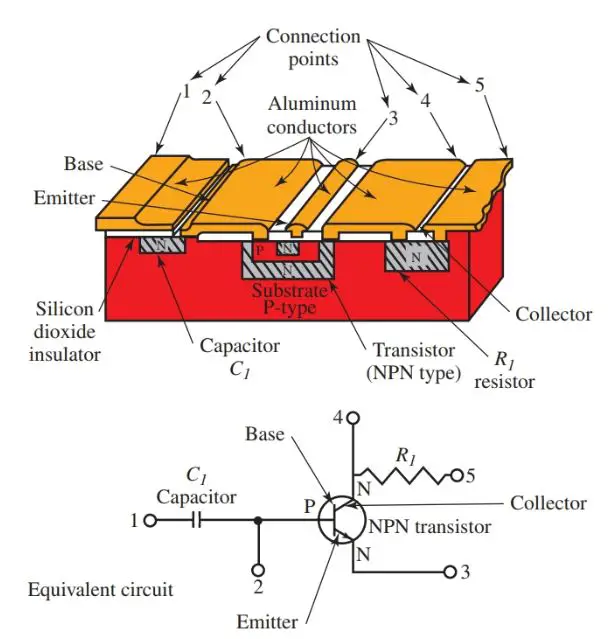
Figure 20. Various components integrated into a small circuit.
Common Types of Integrated Circuits (ICs)
Integrated circuits come in two basic types. The type depends on their function. These types are linear and digital.
Linear ICs have variable outputs, controlled by variable inputs. These ICs are also called analog devices or circuits. Linear ICs are used as components in linear amplifiers, operational amplifiers, voltage regulators/buffers, voltage comparators, analog switches, and audio amplifier circuits.
Digital integrated circuits are used as switches. Their output operates in either on or off conditions. They are found in many logic and gate circuits in computers.
Several IC designs, including pin numbering systems and dimensions, are shown in Figure 21.
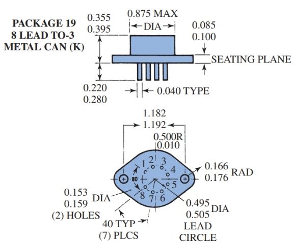
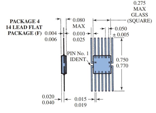
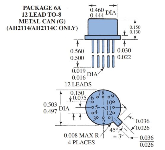
Figure 21. Outlines for several types of ICs. Note the manner in which the pins are numbered. (National Semiconductor)
Integrated Circuit (IC) Key Takeaways
Integrated circuits (ICs) play a vital role in modern electronics due to their compact design, efficiency, and scalability. Their construction—using carefully layered semiconductor materials and photolithography—enables millions of components to function together on a single chip. This advancement has significantly improved the performance and reliability of electronic devices while reducing size and power consumption. ICs are essential in a wide range of applications, from consumer electronics and medical equipment to aerospace systems and advanced computing.