This article outlines standard procedures for testing JFETs and various types of MOSFETs using an ohmmeter.
JFET Testing and Troubleshooting
JFET testing with an ohmmeter is relatively easy. Remember that a JFET is a single bar of silicon with one P–N junction. To identify the leads, first select any two of the three leads. Connect the ohmmeter to these leads. Note the resistance. If it is 100–1000 $\Omega$, the two leads may be the source and drain. Reverse the ohmmeter and connect it to the same leads. If the two leads are actually the source and drain, the same resistance value will be indicated. The third lead is the gate. If the two selected leads show a different resistance in each direction, one must be the gate. Select the third lead and one of the previous leads. Repeat the procedure. A good JFET must show the same resistance in each direction between two leads. This represents the source-drain channel connections.
The gate of a JFET responds as a diode. It will be low resistant in one direction and high resistant in the reverse direction. If the device shows low resistance when the positive probe is connected to the gate and the negative to the source or drain, the JFET is an N-channel device. A P-channel device will show low resistance when the gate is made negative and the source or drain positive. The resistance ratio in the forward and reverse direction must be at least 1:1000 for a good device.
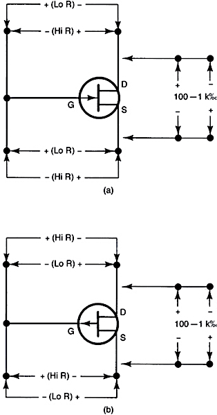
Figure 1. JFET resistance values.
MOSFET Testing
D-MOSFET testing is very similar to the JFET. The gate of the D-MOSFET is insulated from the channel. It will show infinite resistance between each lead regardless of the polarity of the ohmmeter. This is identified by arrows attached to the gate (G).
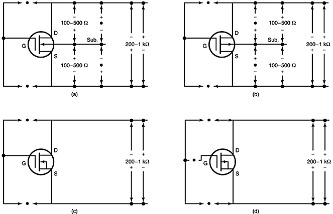
Figure 2. D-MOSFET resistance values.
Three-lead devices have the substrate and source internally connected. Four-lead devices have an independent substrate lead. A four-lead device can be identified as an N-channel or a P-channel device. A P-channel device shows low resistance when the positive lead is connected to the substrate and the negative lead is connected to either the source or drain. An N-channel device has low resistance when the negative lead is connected to the substrate and the positive lead to either the source or drain.
E-MOSFET testing with an ohmmeter is not very meaningful. The structure of this device does not interact effectively between different leads. The gate, source, and drain of a good device show infinite resistance between these leads. A four-lead device responds as a diode between the substrate and the source or drain. The polarity of the ohmmeter can be used to identify the substrate and the channel. A three-lead device responds as a diode between the source and drain.
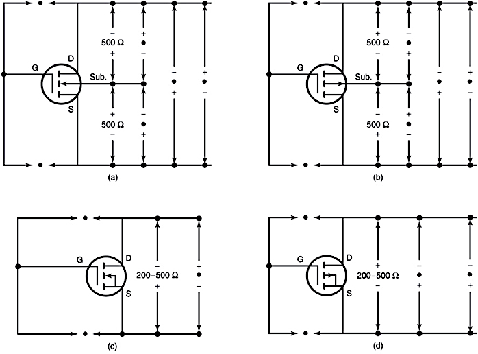
Figure 3. E-MOSFET resistance values.
JFET Fault Diagnosis
JFET troubleshooting is somewhat easy to diagnose because JFETs have only one junction. Shorts and opens may develop across any two terminals. JFETs can be tested without removing them from their circuits. JFET troubleshooting is similar to bipolar junction transistor troubleshooting.
A JFET with a gate-source junction shorted has $V_{GS} \approx 0$ V. As a result, $I_{D}$ will approach $I_{DSS}$. Since there is some gate current, $I_{S}$ and $I_{D}$ will not be equal.
A JFET with an open can be tested by checking two simple conditions:
- $V_{GS} \ne 0$ V
- $I_{D} \ne I_{DSS}$
The operation of a JFET amplifier is shown in Figure 4. It uses only DC sources that are applied to a JFET for setting up its operating conditions. The DC voltage applied sets up the operating conditions. With DC voltage being applied to the gate of the JFET as shown, a measure of whether it is working satisfactorily is determined by the value of the DC across the drain−source voltage, $V_{DS}$. If the DC value of $V_{DS}$ is very low (0 V), it indicates that there might be an internal short between the drain and source terminals. If the DC value of $V_{DS}$ equals the supply voltage, it indicates that there might be an internal open circuit between the drain and source terminals. In either case, the JFET is defective.

Figure 4. JEFT Amplifier Operation – Circuit Diagram
Review Questions
- The resistance between source and drain of a good JFET should be approximately ______ in either direction.
- If the gate of a JFET shows low resistance when the positive probe is connected to it, the JFET is a ______ channel device.
- The gate of a D-MOSFET shows ______ resistance between any two leads.
- A four-lead N-channel D-MOSFET shows low resistance when the ______ lead is connected to the substrate.
- In a JFET, if $V_{DS}$ is 0 V, it may indicate a/an ______ between the drain and source.
- The gate-source junction of a P-channel JFET should conduct when the gate is made ______.
- A working E-MOSFET typically shows ______ resistance between gate, source, and drain.
- For a JFET amplifier, a high $V_{DS}$ value equal to the supply voltage indicates a/an ______ between the drain and source.
Answers
- 100–1000 $\Omega$
- N
- Infinite
- Negative
- Short
- Negative
- Infinite
- Open circuit
Key Takeaways
Understanding and performing proper testing of JFETs and MOSFETs is critical in ensuring the reliability and performance of electronic circuits. These techniques help detect faults early, ensuring efficient operation and reducing the likelihood of component failure in sensitive applications such as amplifiers and switching devices.