The article introduces the concept of sequential logic in digital circuits, focusing on latches and flip-flops as key memory elements. It covers their types, operations, triggering mechanisms, and applications such as counters and frequency dividers.
The goal of this module is to explore Sequential Logic and its functional building blocks and to describe the operations of latches and flip-flops in digital circuits.
Objective
A learner will be able to:
- Explain the difference between combinatorial logic and sequential logic.
- Define positive and negative edge triggering.
- Explain the operation of an SR latch.
- Explain the operation of the gated SR latch.
- Explain the operation of the D Latch.
- Explain the operation of D flip-flops.
- Explain the operation of J/K flip-flops.
- Describe several applications of flip-flops.
- Describe the concept of counting in digital circuits.
- Explain the operation of asynchronous “divide by” counters.
- Explain the operation of synchronous counters.
Orienting Questions
- What is the difference between combinatorial logic and sequential logic?
- How do Latches and flip-flops differ?
- What is positive edge triggering?
- What is negative edge triggering?
- How are flip-flops used in counting and frequency divider circuits?
Introduction
This module will focus on sequential logic. In sequential logic, the output not only depends on the current state of the inputs as combinatorial logic but also on the state of the inputs stored in the past. It can be said that sequential logic is logic with memory. In this module, we will discuss the building blocks of sequential logic which includes latches, and flip-flops. The difference between flip-flops and latches is the way in which the logic changes the state of their outputs. We will also discuss positive and negative edge triggering (trigger) which clocks the way in which the input state changes in sequential circuits.
Latches
Our first adventure into sequential logic is to study latches. A latch is a logic that can “store” a value of 1 or 0 (or a single bit) indefinitely. Latches are in a family of devices known as multivibrators, that is, they are bistable devices that can store 2 stable states. We will discuss the operation of SR (set-reset) latches, gated SR latches and D latch.
SR LATCH
Active high SR latches
This is a latch that will only become activated when one of the inputs momentarily goes high. Active high SR gates can be made from two NOR gates with 1 input of each fed from the output of another. Figure 1 is an illustration of an Active High SR Latch.

Figure 1. Active High SR Latch
The truth table for the active high SR latch is the following:
| S | R | Q | Q’ | |
| 0 | 0 | n/c (latched) | n/c | latched |
| 0 | 1 | 0 | 1 | Reset active high reset command |
| 1 | 0 | 1 | 0 | Set Active high set command |
| 1 | 1 | Invalid | Invalid | Active high on both inputs is invalid
Q = Q’ |
n/c = no change, the latch will stay in whatever state it was in. It will hold its value
invalid = invalid state
You notice from the truth table that if the inputs remain low, the output Q (and Q’) remain unchanged. The only time the outputs change is when one of the inputs momentarily goes high, thus the active high SR latch, this is illustrated in figure 2 below. When S=1, R=0, the latch is in the set state. When S=0, R=1, the latch is in the reset state.
Each time we build or represent this latch, we can represent the Active high SR latch with a block diagram instead of the more complicated NOR gate schematic.
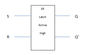
Figure 2. Block diagram SR latch active high
Active low SR latches
Figure 3 below is a latch that will only become activated when one of the inputs momentarily goes low. Active high SR gates can be made from two NAND gates with 1 input of each fed from the output of another.

Figure 3. Active low SR latch
The truth table for the active low SR latch is the following:
| S | R | S’ | R’ | Q | Q’ | |
| 0 | 0 | 1 | 1 | n/c | n/c | latched |
| 0 | 1 | 1 | 0 | 0 | 1 | Reset active low reset command |
| 1 | 0 | 0 | 1 | 1 | 0 | Set Active low set command |
| 1 | 1 | 0 | 0 | invalid | invalid | Active low on both inputs is invalid
Q = Q’ |
n/c = no change, the latch will stay in whatever state it was in. It will hold its value
invalid = invalid state
You notice from the truth table that if the inputs remain low, the output Q (and Q’) remains unchanged. The only time when the outputs change is when one of the inputs momentarily goes low thus the active low SR latch. When S’=1, R’=0, the latch is in the reset state. When S’=0, R’=1, the latch is in the set state. Again, notice that when S’ and R’ are “low”, the latch is set and reset.
We can represent the active low SR latch with a block diagram instead of the more complicated NAND gate schematic each time we build or represent this latch. Figure 4 is an illustration of a Block diagram SR latch active low.
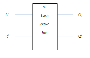
Figure 4. Block diagram SR latch active low
Gated SR latches
If we add a couple of AND gates to the SR latch, we can control, via a third input known as “enable”, when the latch will respond to the inputs S (set) and R (reset). The configuration would look like the image presented in figure 5 below.
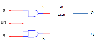
Figure 5. SR gated latch
When the enable input is low, the latch will not respond to any changes in inputs S (set) and R (reset).
When the enable input is high, the S (set) and R (reset) inputs pass through and latch behaves as the SR latch describes in previous two sections.
The truth table for a gated SR latch is the following:
| S | R | EN | Q | Q’ | note |
| 0 | 0 | 0 | NR | NR | No response from the latch. |
| 0 | 1 | 0 | NR | NR | “ |
| 1 | 0 | 0 | NR | NR | “ |
| 1 | 1 | 0 | NR | NR | “ |
| 0 | 0 | 1 | n/c | n/c | Latched |
| 0 | 1 | 1 | 0 | 1 | reset |
| 1 | 0 | 1 | 1 | 0 | set |
| 1 | 1 | 1 | invalid | invalid | Active high on both inputs is invalid
Q = Q’ |
N/C = no change, the latch will stay in whatever state it was in. It will hold its value.
N/R = No response from the latch, that is it remains in whatever state it was in.
D Latch
Another type of gated latch is the D latch. It, just as the gated SR latch, has an enable input which controls when the latch will actually respond to an input. The D latch has only one input as opposed to latches already discussed. The advantage of the D latch is that regardless of the input, there is no invalid state in the output. A schematic diagram of the D Latch is shown below in figure 6.

Figure 6. D latch
The truth table for a D latch is the following:
| D | EN | Q | Q’ | note |
| 0 | 0 | N/R | N/R | No response from the latch |
| 1 | 0 | N/R | N/R | No response from the latch |
| 0 | 1 | 0 | 1 | reset |
| 1 | 1 | 1 | 0 | set |
N/R = No response from the latch, that is it remains it whatever state it was in.
Flip Flops
Flip flops, like latches, are in a family of devices known as multivibrators, that is, they are bistable devices. Flip flops behave similarly to latches except that flip-flops use a clock to change the state of the output. The purpose of the clock is to “trigger” the flip-flop to respond to the inputs. Before we address flip-flops directly, let’s look at what is known as positive and negative edge triggered clock pulses.
Positive and Negative Edge Triggering
Clock signals needed for flip-flops is a waveform which oscillates back and forth between two values. The waveform looks similar to a square wave, however, unlike a pure square wave, the waveform can hold different values for any amount of time. The waveform looks similar to below in figure 7.
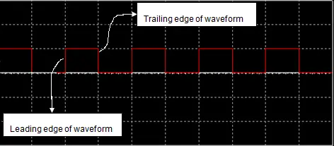
Figure 7. Clock pulse example
As you can see from the waveform above, the clock, as stated before, oscillates between high and low states for some amount of time. It is the leading and trailing edges of the waveform (where the waveform changes) that triggers the input stage. This is known as positive (leading) edge and negative (trailing) edge triggering. Let’s look at some different flip-flops.
D Flip Flops
The first flip-flop we will discuss is the D flip-flop. The D flip-flop operation is similar to the D latch except there is no enable (EN), that is, the positive edge (or negative) edge of the input clock waveform will trigger the flip-flop to respond. We can represent the D flip-flops with schematics. Below in figure 8, you will see an example of the positive and negative edge triggered D-flip flops.
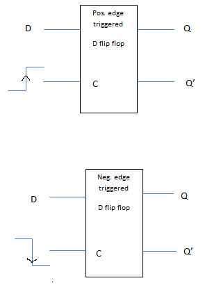
Figure 8: Positive and negative edge triggered D-flip flops
The operation of the D flip-flop is simple. If the D input is high (1) and the clock pulse is positive going (negativoutputsg if negative edge triggered), Q output is high or SET. If the D input is low (0) and the clock pulse is positive going (negative going if negative edge triggered), Q output is high or RESET.
The truth table for the positive edge triggered D flip-flop is the following:
| D | C (clock pulse) | Q | Q’ | |
| 0 | ↑ | 0 | 1 | RESET |
| 1 | ↑ | 1 | 0 | SET |
The truth table for the negative edge triggered D flip-flop is the following:
| D | C (clock pulse) | Q | Q’ | |
| 0 | ↓ | 0 | 1 | RESET |
| 1 | ↓ | 1 | 0 | SET |
J-K Flip Flops
We will now investigate the two input J-K flip-flop operation. Instead of one control input, as the D flip-flop, the J-K flip-flop has two control inputs. The two types of J-K flip-flops we will discuss are synchronous and asynchronous. Asynchronous J-K flip-flops have 2 additional inputs that are independent of the clock pulse.
Synchronous J-K flip flops
The synchronous J-K flip-flop is one that uses a clock to trigger an output based on the state of the two inputs J and K. As with the D flip-flop, it is the leading edge or the negative edge of the clock pulse that triggers the flip-flop to respond to the inputs. For illustrative purposes, we will discuss only the positive edge triggered J-K flip-flop. The operation of the negative edge triggered flip-flop is the same but, as already stated, the output is triggered on the negative edge of the clock pulse.
We can represent the synchronous J-K flip-flop with the following schematic as seen below in figure 9.

Figure 9. Synchronous J-K flip-flop
The operation of the J-K flip-flop is simple. When the appropriate clock pulse is applied, When J and K are low, the outputs are in a latched state, that is, they will not change from their previous state. When J is high and K is low, Q is high, and Q’ is low, that is, it will be SET. When J is low, and K is high, Q is low, and Q’ is high, that is, it is RESET. When both J and K are high, the output will toggle between the SET and RESET states. The toggle will occur with each clock pulse. Toggle modes are used in frequency dividers discussed later in this module.
The truth table for the synchronous J-K flip-flop (assuming positive edge triggered) flip-flop is the following:
| J | K | C | Q | Q’ | |
| 0 | 0 | ↑ | N/C | N/C | No change
Latched |
| 0 | 1 | ↑ | 0 | 1 | RESET |
| 1 | 0 | ↑ | 1 | 0 | SET |
| 1 | 1 | ↑ | Changes | State | Toggle |
Asynchronous J-K Flip Flops
Most J-K flip-flops have two additional inputs which when active will override the J and K (clock driven) inputs. These two inputs are referred to as the PRE (Direct SET) and CLR (Direct Set) inputs. Look at figure 10 below this is a picture of low JK flip-flop. The asynchronous JK flip-flop is on which the outputs are controlled directly with the PRE and CLR inputs and independent of the clock pulse. The PRE and CLR inputs are referred to as asynchronous inputs and when high, take priority over the synchronous inputs J and K. The schematic representation for the asynchronous J-K flip-flop is:
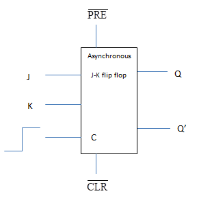
Fig. 10 Asynchronous Active low JK flip-flop
The truth table for the active low asynchronous J-K flip-flop is the following:
| $\overline{PRE}$ | $\overline{CLR}$ | Q | Q’ | |
| 0 | 1 | 1 | 0 | Direct Set |
| 1 | 0 | 0 | 1 | Reset |
| 0 | 0 | Depends on | Clock driven | J-K inputs |
Note: The $\overline{PRE}$,$\overline{CLR}$ and inputs are always active high when clock driven J-K inputs are used. Some flip-flops are active high, that is, they do not use negative logic. They are marked simply PRE and CLR.
The truth tables for this type of active high asynchronous flip-flop is the following:
| PRE | CLR | Q | Q’ | |
| 1 | 0 | 1 | 0 | Direct Set |
| 0 | 1 | 0 | 1 | Reset |
| 0 | 0 | Depends on | Clock driven | J-K inputs |
Note: The PRE and CLR inputs should be active low when clock driven J-K inputs are used.
Application of flip flops
Flip flops can be used in a wide variety of applications. For this module, we will focus on flip-flops as counters and frequency division.
Synchronous Counters
The first counter we will discuss is the synchronous counter. A synchronous counter is one where all of the flip-flops are triggered (clocked) by a common clock. A schematic diagram of a 2 bit synchronous counter is the following:
The synchronous counter works as follows. The clock will trigger an output from the flip-flops. The clock is negative edge triggered as depicted by the bubble on the clock input of each flip-flop. Initially, both outputs of the lamp shown are 0, that is the first clock pulse has not occurred. At the first trigger of the clock, J and K inputs to U3 are high. Output LSB will be high. The second trigger of the clock output of U3 will toggle low and output of U4 will go high, therefore output MSB will be high and LSB will be low. At the third clock pulse, U3 will toggle back high, an output of U4 will remain high, therefore LSB and MSB will be high. And finally, after the fourth clock pulse, both outputs of U3 and U4 will toggle back to zero. LSB and MSB will return to original state.
Note since the PRE and CLR are active low inputs, in order for the counter in figure 11 which is shown below to work, those inputs must be high. It is omitted in this schematic.
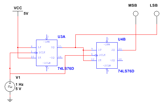
Figure 11. 2-bit Synchronous Counter
Asynchronous Counter
The second counter we will discuss is the asynchronous counter. For this type of counter, the clock drives only the first flip-flop. The remaining flip-flops are triggered by the proceeding flip-flop instead of all the flip-flops triggered by the same clock as described in the previous section on synchronous counters. The schematic diagram for a 2-bit asynchronous clock is the following:
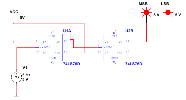
Figure 12. 2-bit Asynchronous Counter
Note: The CLR and PRE set terminals are active low as shown in figure 12 above schematic. These would need to be tied to +5V to inactivate those inputs. They are omitted in this schematic
Operation of the asynchronous counter is as follows:
| Clock pulse (neg. edge triggered in this case) | MSB | LSB | |
| 0 | 0 | Initial conditions | |
| 1 | 0 | 1 | |
| 2 | 1 | 0 | |
| 3 | 1 | 1 | |
| 4 | 0 | 0 | Resets |
As you can see, the counter will count to binary up to 3, and on the fourth clock pulse the counter will reset and begin the count all over again.
Frequency Division
One final application of flip-flops that we will discuss in this module is frequency division. Below in figure 13, you will see a picture of this. As already noted, when PRE and CLR asynchronous inputs are disabled, and inputs J and K are held High, the output of the flip-flop, Q (and Q’) will toggle between high (1) and Low (0) states on the leading or trailing edge of the clock input pulse. When this happens, the output frequency of the flip-flop is half the input clock frequency. See circuit and subsequent output display below
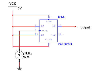
Figure13. Simple Frequency Divider
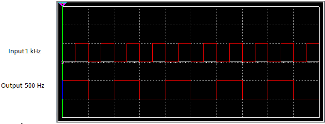
Figure 14. The output of Frequency Divider
As you can see, the output of the flip-flop is 500 Hz or one half the input clock frequency as seen in figure 14 above.
Let’s work an example problem and expand our knowledge of frequency dividers.
Create a frequency divider using J-K flip-flops whose input frequency is 4 kHz and output is 1 kHz. Look at figure 15 for a detailed picture.
Solution:
From the information given in the problem, the output of 1kHz is 4 times less than the input frequency, therefore, this is a divide by 4 dividers. A single flip-flop will divide the frequency by 2, therefore, we must have 2 flip-flops to divide by 4. The design and output is as follows

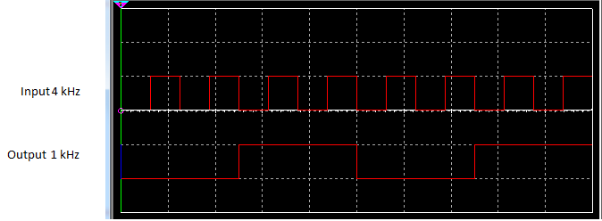
Figure 15. Frequency Input and Output Divider
Therefore the configuration of the frequency divider is the same as the asynchronous counter. For each flip-flop added to the circuit, the frequency is reduced by a half. The frequency division can be written as
\[{{f}_{out\text{ }=}}\frac{{{f}_{in}}}{{{2}^{n}}}\]
where n = number of flip flops
Latches and Flip Flops Key Takeaways
Understanding latches and flip-flops is essential in the field of digital electronics because they form the foundational building blocks of sequential logic circuits. These memory elements enable circuits to store and manipulate binary information based on past and present inputs, which is crucial for designing systems that require memory and state transitions. Applications such as counters and frequency dividers rely heavily on the precise behavior of flip-flops and latches, allowing digital systems to keep track of events, synchronize data, and perform time-based operations. These functions are vital in a wide range of technologies, including digital clocks, microprocessors, communication systems, and control units.