In this article, we will learn about the operation of AND, OR, and NOT logic gates and their associated truth tables and Boolean expressions.
Objectives
A learner will be able to:
- Explain the difference between analog and digital quantities
- Give examples of binary numbers and describe their structure
- Give examples of hexadecimal and octal number systems and convert between binary, hexadecimal, and octal number systems
- Use a calculator to perform number system conversion and hexadecimal arithmetic
- Describe logic levels used in digital systems and analyze the characteristics of a pulse waveform
- Discuss the elements that make up a digital system
Orienting Questions
- What are the basic logic gates that are the basic building blocks for all logic circuits?
- What are the schematic symbols of the AND, OR, and NOT logic gates?
- What is Boolean Algebra?
- How do you apply Boolean Algebra to circuits containing AND, OR, and NOT logic gates?
- What are the schematic symbols for NAND and NOR logic gates?
- How do you apply Boolean Algebra to circuits containing NAND and NOR logic gates?
Introduction
The building blocks of all logic gates are the AND, OR, and NOT logic gates. In this article, we will explore the operation of each of these logic gates. We will also introduce Boolean Algebra, which describes the operation of all logic gates and gate combinations. At the end of the article, we will introduce the NAND(Not AND) and NOR(Not OR) gates and introduce their Boolean expressions as well.
AND, OR, NOT Gates
In this section, we will learn about the operation of AND, OR, and NOT logic gate functions and their associated truth tables and Boolean expressions.
AND Gate
All digital systems operate in binary, that is, they have two distinctive states or levels. These states or levels can be referred to as 0 or 1, high or low, on or off, true or false, the possibilities are endless. These states or levels describe a relationship between inputs and outputs. We can represent the most basic logic gates (AND and OR) as equivalent to the most basic types of circuits, that is, series and parallel.
AND gate operation is similar to a basic series circuit as shown in Figure 1 below. The inputs are represented by the switches sw1, and sw2 and the output is represented by the lamp. The “state” of sw1 and sw2 determines whether or not the lamp illuminates. It is easy to see that the only condition for which the lamp is on is that sw1 and sw2 must be closed. We can represent all possible states or conditions of sw1 and sw2 and the associated output through a truth table.
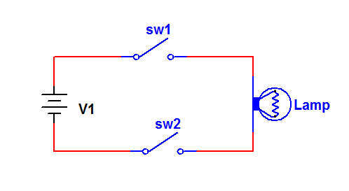
Figure 1. Series Circuit
Note that the number of input combinations depends on the number of switches in this case. We can write a general expression for this as follows
Number of to input states = 2n
Where n = number of inputs
Therefore, a truth table for this setup would look like the following:
| SW1 | SW2 | Bulb |
| Open | Open | Off |
| Open | Closed | Off |
| Closed | Open | Off |
| Closed | closed | on |
This series circuit configuration is the equivalent of the basic AND gate. The AND gate is then defined as a digital circuit whose output is “high” if and only if all inputs are “high”.
The schematic representation of an AND gate in digital circuits is:
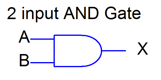
Figure. 2-Input AND Gate Schematic Symbol
A and B are the inputs to the gate, and X is the corresponding output.
Boolean Algebra Truth Table For 2-input AND Gate
The truth table for the 2 input AND gate in terms of Binary numbers is:
| A | B | X |
| 0 | 0 | 0 |
| 0 | 1 | 0 |
| 1 | 0 | 0 |
| 1 | 1 | 1 |
0 = “off” or “low”
1 = “on” or “high”
OR Gate
The next logic gate we will investigate is the operation of the OR gate. OR gate operation is similar to a basic parallel circuit as shown in Figure 2 below. The inputs are represented by the switches sw1, and sw2 and the output is represented by the lamp. The “state” of sw1 and sw2 determines whether or not the lamp illuminates. The conditions for which the lamp is on is that sw1 or sw2, or sw1 and sw2 must be closed. We can represent all possible states or conditions of sw1 and sw2 and the associated output through a truth table.
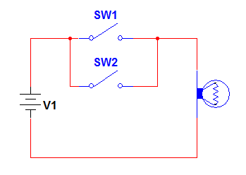
Figure 2. Basic parallel Circuit
Note that the number of input combinations depends on the number of switches in this case. We can write a general expression for this as follows:
Number of to input states = 2n
Where n = number of inputs
Therefore, a truth table for this setup would look like the following:
| SW1 | SW2 | Bulb |
| Open | Open | Off |
| Open | Closed | on |
| Closed | Open | on |
| Closed | closed | on |
This parallel circuit configuration is the equivalent of the basic OR gate. The OR gate is then defined as a digital circuit whose output is “high” if one or more inputs are “high”.
The schematic representation of an OR gate in digital circuits is:
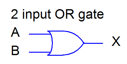
Figure 3. OR Gate Schematic Symbol in Digital Circuits
A and B are the inputs to the gate, and X is the corresponding output.
Boolean Algebra Truth Table For 2-input OR Gate
The truth table for the 2 input OR gate in terms of Binary numbers is:
| A | B | X |
| 0 | 0 | 0 |
| 0 | 1 | 1 |
| 1 | 0 | 1 |
| 1 | 1 | 1 |
0 = “off” or “low”
1 = “on” or “high”
NOT Gate
The last basic logic gate we will investigate is the NOT gate and its operation. The operation of the NOT gate is sometimes referred to as an inverter, that is, it inverts or changes a single logic level to the opposite value. So an input of “0” yields an output of “1”, and an input of “1” yields an output of “0”.
The schematic symbol for the inverter (NOT Gate) is as follows.
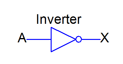
Figure 4. Schematic Symbol for the Inverter (NOT Gate)
The bubble on the end indicates an inversion of A!
Boolean Algebra Truth Table For NOT Gate
An inverter only has one input and one output. That is, it operates only on one variable. The truth table for the inverter is:
| A | X |
| 0 | 1 |
| 1 | 0 |
0 = “off” or “low”
1 = “on” or “high
The output of the inverter is the complement (opposite) of the input. It can be stated that output is the not of the input. We will discuss the Boolean expression of the NOT gate in the next section.
Boolean Algebra of AND OR And NOT Logic Gates
Boolean algebra represents the mathematics of Digital Electronics Circuits. The operation of any logic gate or combination of logic gates can be described using Boolean algebra. In this section, we will look at Boolean algebra of the basic gates already discussed and address the basic Boolean rules (laws). We will also begin to draw circuits from un-simplified Boolean expressions.
AND Gate
The AND gate represents Boolean multiplication, that is, the AND’ing or product of 2 inputs results in the output. Recall the truth table for the AND gate
| A | B | X |
| 0 | 0 | 0 |
| 0 | 1 | 0 |
| 1 | 0 | 0 |
| 1 | 1 | 1 |
As already stated it has been shown that the AND operator is referred to as Boolean multiplication. The Boolean expression for this operation is given below.
A*B = X
AB = X
We will use the latter as the notation for Boolean multiplication from here on. The correct way to state this is “A and B = X”
When we take the product of two variables, the order in which the input variables are multiplied together does not affect the result. That is
AB = BA Commutative Law for multiplication
OR Gate
The OR gate represents Boolean addition, that is, the OR’ing or sum of 2 inputs results in the output. Recall the truth table for the OR gate.
| A | B | X |
| 0 | 0 | 0 |
| 0 | 1 | 1 |
| 1 | 0 | 1 |
| 1 | 1 | 1 |
Remember we are not adding the two numbers, we are performing the “operation” between them. We are performing Boolean addition and not basic arithmetic.
As already stated it has been shown that the OR operator is referred to as Boolean addition (+). The Boolean expression for this operation is given below.
A + B = X
Properly stated “A or B = X”
When we take the Boolean sum of two variables, the order in which the input variables are summed does not affect the result. That is
A + B = B + A Commutative Law for addition
NOT Gate
As already stated, the NOT gate represents Boolean complement, that is, the inversion of a single input results in the output. Recall the truth table for the NOT gate
| A | X |
| 0 | 1 |
| 1 | 0 |
A = 1, X = 0
A = 0, X = 1
The Boolean expression for this operation is given
$\overline{A}$=X
Properly stated “A Not = X”
When we take the complement of a single variable, the output is the opposite of the input.
Basic Boolean Rules
Shown below in Figure 5 is how each logic gate would be represented in terms of its Boolean expression (as opposed to just X!). We will now write some Boolean rules associated with each of these basic gates. We will apply these rules throughout our study of combinatorial logic.
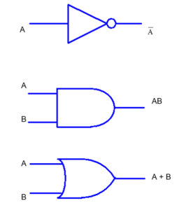
Figure 5. Basic Logic Gates Representation
Some basic Boolean Rules:
- AB = BA Commutative Law for multiplication
- A + B = B + A Commutative Law for addition
- A ∙ 0 = 0
- A ∙ 1 = A
- A ∙ A = A
- A + 0 = A
- A + 1 = 1
- A + A = A
- A ∙ = 0
- A + = 0
- = A
- A + AB = A
- A + B = A + B
- (A+B)(A+C) = A + BC
NAND and NOR Gates
We can combine any of the basic gates AND, OR, and NOT to create new logic circuits with unique outputs. In this section, we will investigate the operation of NAND (Not AND) and NOR (Not OR) gates and their associated schematics and Boolean expressions.
NAND GATE
When we have an AND gate and follow it with an inverter, we have a NAND gate.
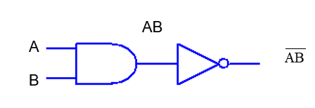
Figure 6. NAND Gate
By combining the AND and NOT gates this way, we have created a unique gate which has its own unique outputs for given inputs. The truth table would then look like this
| A | B | AB | $\overline{AB}$ |
| 0 | 0 | 0 | 1 |
| 0 | 1 | 0 | 1 |
| 1 | 0 | 0 | 1 |
| 1 | 1 | 1 | 0 |
We can replace the above 2 gates with an equivalent NAND gate.
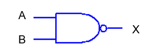
Figure 7. Schematic Symbol for NAND Gate
Note: the NAND schematic symbol is simply the AND gate with the negation symbol on its output
The truth table for the NAND gate is
| A | B | X |
| 0 | 0 | 0 |
| 0 | 1 | 1 |
| 1 | 0 | 1 |
| 1 | 1 | 1 |
NOR GATE
When we have an OR gate and follow it with an inverter, we have a NOR gate.
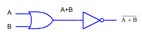
Figure 8. NOR Gate Symbol
By combining the OR and NOT gates this way, we have created a unique gate which has its own unique outputs for given inputs. The truth table would then look like this
| A | B | A+B | $\overline{A+B}$ |
| 0 | 0 | 0 | 1 |
| 0 | 1 | 1 | 0 |
| 1 | 0 | 1 | 0 |
| 1 | 1 | 1 | 0 |
We can replace the above 2 gates with an equivalent NOR gate.
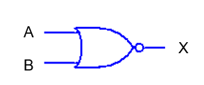
Figure 9. Schematic Symbol for NAND Gate
Note: the NOR schematic symbol is simply the OR gate with the negation symbol on its output.
The truth table for the NOR gate is:
| A | B | X |
| 0 | 0 | 1 |
| 0 | 1 | 0 |
| 1 | 0 | 0 |
| 1 | 1 | 0 |
Basic Logic Gates and Boolean Expressions Key Takeaways
Understanding the operation of AND, OR, and NOT logic gates, along with their truth tables and Boolean expressions, is crucial in the field of digital electronics. These basic logic gates form the foundation for all complex digital systems, from simple circuits to advanced computing devices. Their real-world applications are vast—ranging from decision-making circuits in microprocessors to control systems in automation, and from data routing in communication systems to logic controllers in industrial electronics.