This article introduces the concept of Enhancement MOSFETs (E-MOSFET). It covers their internal structure, operating principles, voltage characteristics, and the drain family of characteristic curves essential for understanding their role in amplification and switching applications.
Metal-Oxide Semiconductor Field-Effect Transistors (MOSFETs) are widely used semiconductor devices known for their high input impedance and efficient switching behavior. Unlike Bipolar Junction Transistors (BJTs), which are current-controlled devices, MOSFETs are voltage-controlled, requiring very little input current at the gate. They also differ from Junction Field-Effect Transistors (JFETs), which have a built-in channel and operate with reverse-biased gate voltage. MOSFETs offer better scalability and integration into digital and analog circuits, making them ideal for modern electronics.
There are two main types of MOSFETs: Depletion-type and Enhancement-type, each with distinct characteristics. This article discusses the structure, operation, and characteristic curves for E-MOSFETs.
E-MOSFET Structure
An enhancement metal-oxide semiconductor field-effect transistor (E-MOSFET) is a type of MOSFET in which current carriers are pulled from the substrate to form an induced channel. The channel is produced only when the device is energized. Gate voltage is used to control the size of the induced channel. An E-MOSFET is classified as a normally off device.
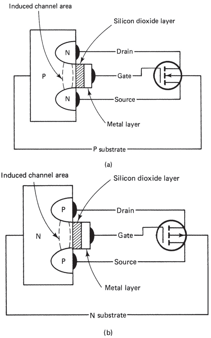
Figure 1. E-MOSFET crystal structures, element names, and schematic symbols. (a) P-channel E-MOSFET. (b) N-channel E-MOSFET.
Figure 1 shows a cross-sectional view of the crystal structure, element names, and schematic symbols of the P-channel and N-channel E-MOSFETs. Note that a defined channel connection does not exist between the source and drain. The entire device is built on a piece of semiconductor material called the substrate. Gate construction is designed to span the entire space between the source and drain. A thin layer of metal is used in the construction of the gate.
The schematic symbol shows this by having independent source, substrate, gate, and drain leads. The middle electrode, which has an arrowhead, shows the polarity of the substrate. When the arrow points in toward the channel, it indicates that the substrate is P-type material and the channel is N-type material, as in Figure 1(b). When the arrow does not point toward the channel, it shows that the substrate is N-type material and the channel is P-type material, as shown in Figure 1(a).
E-MOSFET Operation
The operation of an E-MOSFET is primarily based on the voltage value and polarity of its elements. Look at the circuit diagrams in Figure 2, which illustrate the correct voltage polarity for N-channel and P-channel E-MOSFETs. In the circuit, cross-sectional crystal structure views are also included to illustrate the formation of the induced channels.
Note in Figure 2(a) that when the gate of an N-channel device is made positive, electrons are pulled from the P substrate into the source-drain region. This condition causes the channel region to have a high concentration of current carriers. Completion of the channel provides a conduction path for current carriers to flow between the source and drain. The drain current, in effect, is aided or enhanced by the gate voltage ($V_{G}$). The absence of gate voltage does not permit the channel to form. The size of the channel and density of the current carriers are directly related to the value of $V_{G}$.
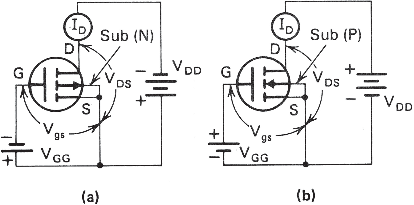
Figure 2: E-MOSFET voltage polarities. (a) P-channel. (b) N-channel.
Now, take a look at Figure 2(b). Note that the P-channel device has the source and drain energized by $V_{DD}$. The source is positive, and the drain is negative. The gate is made negative with respect to the source by battery $V_{GG}$. A negative gate pulls holes from the N substrate, forming the induced P-channel. Current flow through the channel is achieved by hole movement. The P–N junction formed by the P-type source and drain and the N-type substrate must be reverse-biased. The substrate of both P-channel and N-channel MOSFETs is usually connected to the same polarity as the source.
E-MOSFET Characteristic Curves
A drain family of characteristic curves for an E-MOSFET is shown in Figure 3. This set of curves is for an N-channel device. A set of curves for a P-channel device would be very similar. The primary difference is the polarity of the gate voltage. Note that an increase in $V_{GS}$ causes a corresponding increase in drain current. Individual curves represent different values of $V_{GS}$. Increasing $V_{DS}$ also causes an increase in $I_{D}$. The leveling off of $I_{D}$ indicates the pinch-off region of the device. The pinch-off region and the ohmic region of this device are similar to those of the JFET.
A drain family of characteristic curves of this type could be used to develop a load line for a representative amplifier. The procedure of creating a load line for an E-MOSFET amplifier is primarily the same as that for a JFET.
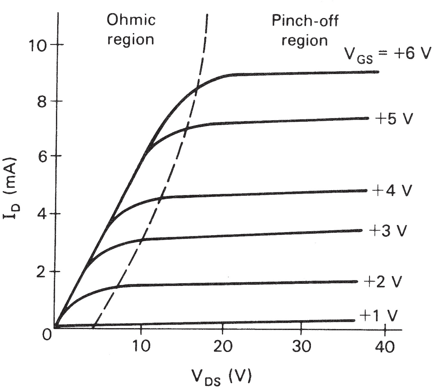
Figure 3. A drain family of characteristic curves for an N-channel E-MOSFET.
Review Questions
- An E-MOSFET is classified as a _______ device.
- The channel in an E-MOSFET is formed only when _______ is applied.
- In an N-channel E-MOSFET, the gate must be made _______ to induce a channel.
- The P-channel E-MOSFET uses a _______ gate voltage to form the channel.
- The current in an N-channel E-MOSFET is carried by _______.
- The leveling off of $I_{D}$ in the characteristic curves represents the _______ region.
- The gate construction in an E-MOSFET spans the area between _______ and _______.
- The schematic symbol for an E-MOSFET includes leads for source, gate, drain, and _______.
- The size of the induced channel is directly related to the value of _______.
- The drain family of curves helps in developing a _______ line for amplifier analysis.
Answers
- normally off
- gate voltage
- positive
- negative
- electrons
- pinch-off
- source, drain
- substrate
- $V_{G}$
- load
Key Takeaways
E-MOSFETs play a critical role in modern electronics due to their efficient switching capabilities and low power operation. Understanding their structural design, operational principles, and output characteristics is essential for analyzing and designing amplifier and switching circuits.