This article provides an overview of Junction Field-Effect Transistors (JFETs), covering their construction, operation, and the differences between N-channel and P-channel JFETs.
Junction Field-Effect Transistors (JFETs)
A transistor that has only one P–N junction in its construction is called a unipolar transistor. Unlike the bipolar transistor, which has two P–N junctions, a unipolar transistor conducts current through a single piece of semiconductor material. Current carriers passing through this material can be either electrons or holes, depending on the polarity of the semiconductor. Field-effect transistors (FETs) are unipolar devices. These devices represent a unique part of the semiconductor field.
An FET is primarily a three-terminal device that is capable of amplification, switching, and most of the functions of a bipolar transistor. FETs are used as discrete devices or can be fabricated into integrated circuits. FETs fall into two general classifications: Junction Field-Effect Transistor (JFET) and Insulated Gate Field-Effect Transistor (IGFET). The JFET was developed first.
Two Types of JFET
The Junction Field-Effect Transistor (JFET) is a three-element electronic device. Its operation is based on the conduction of current carriers passing through a single piece of semiconductor material instead of a junction. The two major types of JFETs are N-channel and P-channel. JFET circuit operation can be predicted with a family of characteristic curves and a dynamic transfer curve.
N-Channel JFET
The crystal structure, element names, and schematic symbol of an N-channel JFET are shown in Figure 1. It is constructed of a block of N-type material. The P-type material of the gate is then diffused into the N channel. Lead wires attached to each end of the channel are the source (S) and drain (D) connections. The gate lead is attached to the diffused P-material.
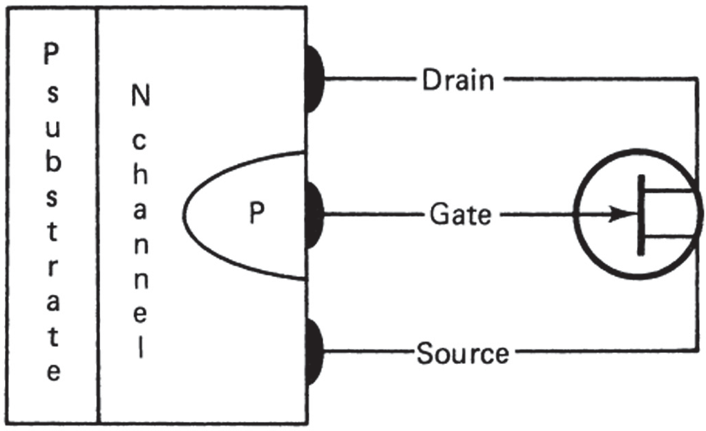
Figure 1. N-Channel JFET crystal structure and symbol.
The schematic symbol of an N-channel JFET is somewhat representative of its construction. The bar part of the symbol refers to the channel. The drain and source leads are attached to the channel. The gate (G) has an arrow. This shows that it forms a P–N junction. The arrowhead of an N-channel symbol points in toward the channel, indicating that it is a P–N junction. The gate is a P-type material, and the channel is an N-type material. This part of the device responds as a P–N junction diode.
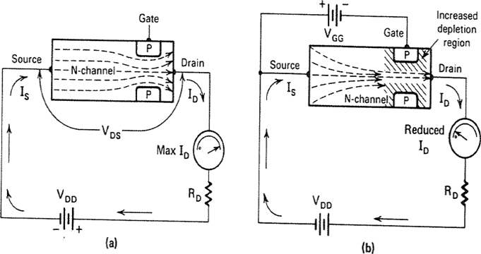
Figure 2. N-channel JFET: (a) crystal structure, element names; (b) Biasing.
The operation of a JFET is somewhat unusual when compared with that of a bipolar transistor. Figure 2 shows a cross-sectional view of a JFET in a circuit. The source and drain leads of the JFET are connected to a DC voltage source. In this case, maximum current flows through the channel. This is called drain current (ID). The value of VDD and the internal resistance of the channel determine the amount of channel current flow (ID). Typical source-drain resistance values of a JFET are several hundred ohms, meaning that full conduction takes place in the channel even when the gate is open. A JFET is, therefore, considered to be a normal-on device.
The amount of bias voltage applied to the gate controls the current carriers passing through the channel of a JFET. In normal circuit operation, the gate is reverse-biased with respect to the source. Reverse biasing of the gate-source junction increases the size of its depletion region, which restricts or depletes the number of majority carriers that can pass through the channel. This means that ID is controlled by the value of the gate-source voltage (VGS). If VGS becomes great enough, no ID will be permitted to flow through the channel. The voltage that causes this condition is called the cutoff voltage. ID can be controlled anywhere between full conduction and cutoff by a small change in gate voltage.
Figure 2 (b) shows how the JFET responds when VDD and VGG are connected simultaneously. Note that the gate−source junction is reverse-biased by the VGG battery. This voltage increases the size of the depletion region near the gate. As a result, the number of current carriers in the channel is reduced. An increase in VGS causes a corresponding decrease in ID. Reducing the value of VGS causes a substantial increase in ID. Thus, a change in the value of VGS can be used to control the internal resistance of the channel. Variations in VGS are, therefore, used to control channel current, or ID.
P-Channel JFET
The crystal structure, element names, and schematic symbol of a P-channel JFET are shown in Figure 3. This device is constructed with a block of P-type material. The N-type material of the gate is diffused into the P-channel. Leads are attached to each end of the channel and to the gate. Other construction details are the same as those of the N-channel device.
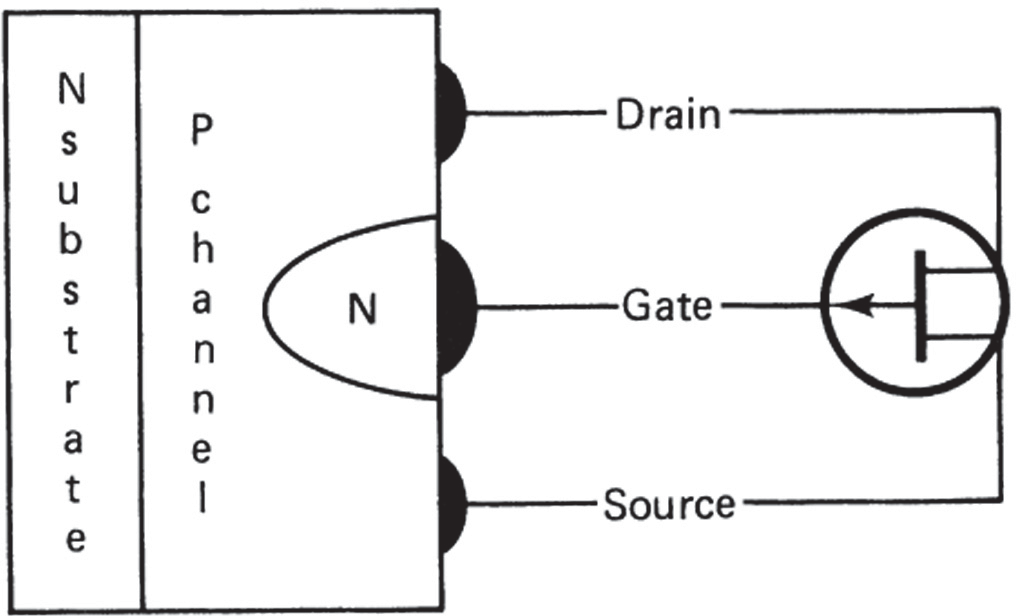
Figure 3. P-channel JFET crystal structure, element names, and schematic symbol.
The schematic symbol of a JFET is different only in the gate element. In a P-channel device, the arrow does not point toward the channel. This means that the gate is N-type material, and the channel is P-type material. In the conventional operation of a P-channel JFET, the gate is made positive with respect to the source. Varying values of the reverse-bias gate voltage change the size of the P–N junction depletion zone. Current flow through the channel can be altered between cutoff and full conduction. P-channel and N-channel JFETs cannot be used in a circuit without changing the polarity of the voltage source.
Review Questions
- A Junction Field-Effect Transistor (JFET) operates based on the conduction of current carriers through a __________ piece of semiconductor material.
- The two major types of JFETs are __________ and __________.
- In an N-channel JFET, the gate is a __________ material, and the channel is a __________ material.
- The JFET is considered a __________-on device when the gate is open.
- The __________ voltage causes the condition where no current flows through the channel of a JFET.
- In a P-channel JFET, the gate is __________ with respect to the source.
- The drain current (ID) in a JFET is controlled by the __________ voltage.
- The operation of a JFET is based on the conduction of current carriers through a __________ piece of semiconductor material.
- The cutoff voltage in a JFET refers to the value of __________ when no current flows through the channel.
- In a P-channel JFET, the gate arrowhead does not point __________ the channel.
Answers
- Single
- N-channel, P-channel
- P-type, N-type
- Normal
- Cutoff
- Positive
- Gate-source
- Single
- Gate-source voltage
- Toward
Key Takeaways
Junction Field-Effect Transistors (JFETs) are essential devices in modern electronics, particularly for controlling current flow in circuits. Both N-channel and P-channel JFETs serve specific roles, with the current conduction controlled via gate voltage.