The article discusses key signal processing applications of diodes, including the diode clipper (limiter), diode clamp, and peak detector. It highlights how the non-linear characteristics of diodes enable these circuits to modify, shift, or detect signal waveforms.
Among the numerous applications of diodes, there are a number of interesting signal conditioning or signal processing applications that are made possible by the non-linear nature of the device. We explore three such applications here: the diode limiter, or clipper; the diode clamp; and the peak detector. Other applications are left for the homework problems.
Diode Clipper (Limiter)
The diode clipper is a relatively simple diode circuit that is often employed to protect loads against excessive voltages. The objective of the clipper circuit is to keep the load voltage within a range, say, −Vmax ≤ υo(t) ≤ Vmax, so that the maximum allowable load voltage (or power) is never exceeded. The circuit of Figure 1 accomplishes this goal.
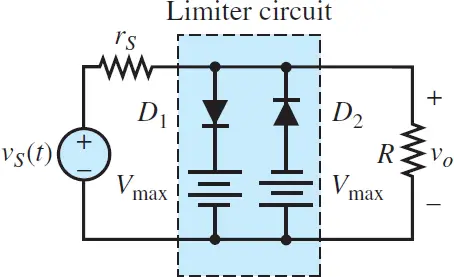
Figure 1 Two-sided diode clipper
The circuit of Figure 1 is most easily analyzed by first considering just the branch containing D1. This corresponds to clipping only the positive peak voltages; the analysis of the negative voltage limiter is left as a drill exercise. The circuit containing the D1 branch is sketched in Figure 2; note that we have exchanged the location of the D1 branch and that of the load branch for convenience.
Further, the circuit is reduced to Thevenin equivalent form. Having reduced the circuit to a simpler form, we can now analyze its operation for two distinct cases: the ideal diode and the piecewise linear diode.
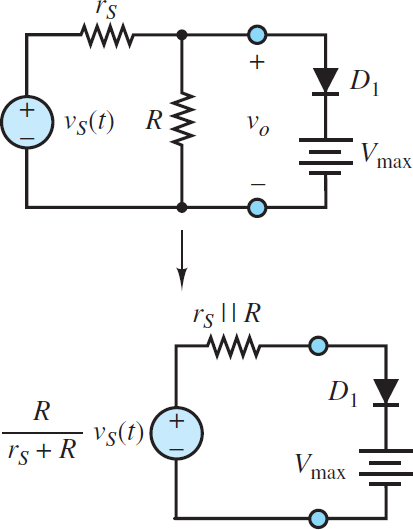
Figure 2 Circuit model for the diode clipper
1. Ideal diode model. For the ideal diode case, we see immediately that D1 conducts if
\[\frac{R}{{{r}_{S}}+R}{{v}_{S}}(t)\ge {{V}_{\max }}\begin{matrix}{} & {} & (1) \\\end{matrix}\]
and that if this condition occurs, then (D1 being a short-circuit) the load voltage υo becomes equal to Vmax. The equivalent circuit for the on condition is shown in Figure 3.
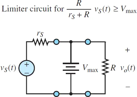
Figure 3 Equivalent circuit for the one-sided limiter (diode on)
If, on the other hand, the source voltage is such that
\[\frac{R}{{{r}_{S}}+R}{{v}_{S}}(t)<{{V}_{\max }}\begin{matrix}{} & {} & (2) \\\end{matrix}\]
then D1 is an open-circuit and the load voltage is simply
\[{{v}_{0}}(t)=\frac{R}{{{r}_{S}}+R}{{v}_{S}}(t)\begin{matrix}{} & {} & (3) \\\end{matrix}\]
The equivalent circuit for this case is depicted in Figure 4.
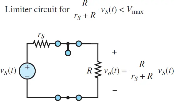
Figure 4 Equivalent circuit for the one-sided limiter (diode off)
The analysis for the negative branch of the circuit can be conducted by analogy with the preceding derivation, resulting in the waveform for the two-sided clipper shown in Figure 5.
Note how the load voltage is drastically “clipped” by the limiter in the waveform of Figure 5. In reality, such hard clipping does not occur, because the actual diode characteristic does not have the sharp on/off breakpoint the ideal diode model implies. One can develop a reasonable representation of the operation of a physical diode limiter by using the piecewise linear model.
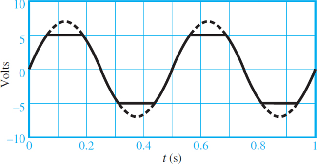
Figure 5 Two-sided (ideal diode) clipper input and output voltages
2. Piecewise linear diode model. To avoid unnecessary complexity in the analysis, assume that Vmax is much greater than the diode offset voltage, and therefore assume that Vγ ≈ 0. We do, however, consider the finite diode resistance rD. The circuit of Figure 55 still applies, and thus the determination of the diode on/off state is still based on whether [R/(rS + R)]vS(t) is greater or less than Vmax. When D1 is open, the load voltage is still given by
\[{{v}_{0}}(t)=\frac{R}{{{r}_{S}}+R}{{v}_{S}}(t)\begin{matrix}{} & {} & (3) \\\end{matrix}\]
When D1 is conducting, however, the corresponding circuit is as shown in Figure 6.
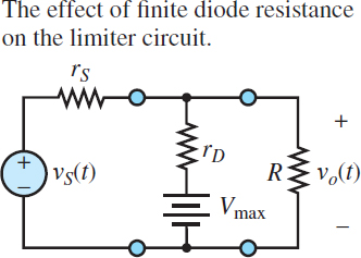
Figure 6 Circuit model for the diode clipper (piecewise linear diode model)
The primary effect the diode resistance has on the load waveform is that some of the source voltage will reach the load even when the diode is conducting. This is most easily verified by applying superposition; it can be readily shown that the load voltage is now composed of two parts, one due to the voltage Vmax and the other proportional to vS(t):
\[{{v}_{0}}(t)=\frac{R\parallel {{r}_{S}}}{{{r}_{D}}+(R\parallel {{r}_{S}})}{{V}_{\max }}+\frac{{{r}_{D}}\parallel R}{{{r}_{S}}+({{r}_{D}}\parallel R)}{{v}_{S}}(t)\begin{matrix}{} & {} & (5) \\\end{matrix}\]
It may easily be verified that as rD → 0, the expression for vo(t) is the same as that for the ideal diode case. The effect of the diode resistance on the limiter circuit is depicted in Figure 7. Note how the clipping has a softer, more rounded appearance.
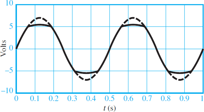
Figure 7 Voltages for the diode clipper (piecewise linear diode model)
Diode Clamp
Another circuit that finds common application is the diode clamp, which permits “clamping” a waveform to a fixed DC value. Figure 8 depicts two different types of clamp circuits.
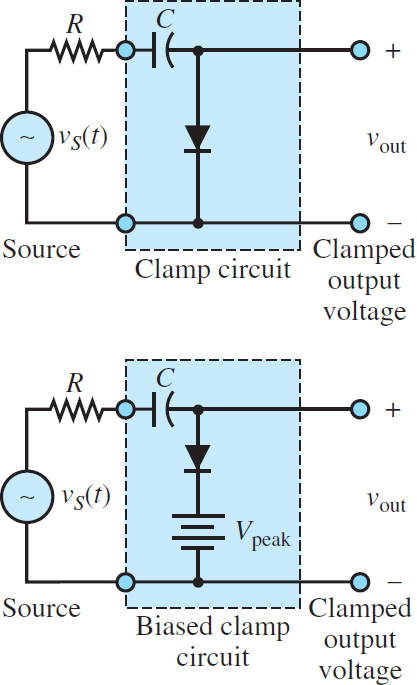
Figure 8 Diode clamp circuits
The operation of the simple clamp circuit is based on the notion that the diode will conduct current only in the forward direction, and that therefore the capacitor will charge during the positive half-cycle of vS(t) but will not discharge during the negative half-cycle. Thus, the capacitor will eventually charge up to the peak voltage of vS(t), denoted by Vpeak. The DC voltage across the capacitor has the effect of shifting the source waveform down by Vpeak, so that after the initial transient period the output voltage is
\[{{v}_{out}}(t)={{v}_{S}}(t)-{{V}_{peak}}\begin{matrix}{} & {} & (6) \\\end{matrix}\]
and the positive peaks of vS(t) are now clamped at 0 V. For equation 30 to be accurate, it is important that the RC time constant be greater than the period T of vs(t):
\[RC\gg T\begin{matrix}{} & {} & (7) \\\end{matrix}\]
Figure 9 depicts the behavior of the diode clamp for a sinusoidal input waveform, where the dashed line is the source voltage and the solid line represents the clamped voltage.
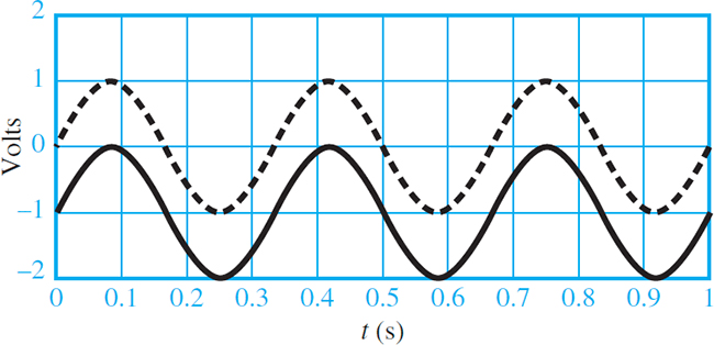
Figure 9 Ideal diode clamp input and output voltages
The clamp circuit can also work with the diode in the reverse direction; the capacitor will charge to −Vpeak with the output voltage given by
\[{{v}_{out}}(t)={{v}_{S}}\left( t \right)+{{V}_{peak}}\begin{matrix}{} & {} & (8) \\\end{matrix}\]
Now the output voltage has its negative peaks clamped to zero since the entire waveform is shifted upward by Vpeak volts. Note that in either case, the diode clamp has the effect of introducing a DC component in a waveform that does not originally have one. It is also possible to shift the input waveform by a voltage different from Vpeak by connecting a battery VDC in series with the diode, provided that
\[{{V}_{DC}}<{{V}_{peak}}\begin{matrix}{} & {} & (9) \\\end{matrix}\]
The resulting circuit is called a biased diode clamp.
Diode Peak Detector
Another common application of semiconductor diodes, the peak detector, is very similar in appearance to the half-wave rectifier with capacitive filtering as shown in Figure 10. One of its more classic applications is in the demodulation of amplitude-modulated (AM) signals.
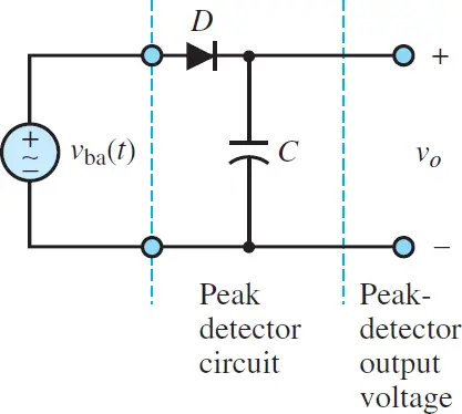
Figure 10 Peak detector circuit
Signal Processing Applications Key Takeaways
The diode clipper, clamp, and peak detector are vital signal processing applications that utilize the nonlinear characteristics of diodes to manipulate electrical signals effectively. These circuits are widely used in electronic systems to protect devices, shift waveform levels, and detect signal peaks—making them indispensable in areas such as communications, instrumentation, and control systems. Understanding these signal processing applications not only highlights the practical versatility of diodes but also demonstrates their crucial role in shaping and interpreting analog signals. As foundational tools in the electronics field, these signal processing applications enable engineers to design circuits that are both functional and reliable in real-world environments.