The major difference between bipolar junction transistor and field-effect transistor (FET) is that the BJT is a current device, and the FET is a voltage device.
The current through the collector-emitter circuit of a BJT is controlled by the amount of current in the base-emitter circuit. A FET controls current in the source-drain circuit by the amount of potential applied to the gate.
Field-Effect Transistor (FET) Types
There are two types of FETs, the junction field-effect transistor (JFET) and the metal oxide semiconductor field-effect transistor (MOSFET). First, we will look at the JFET.
JFET Construction
The construction and symbols for the JFET are shown in Figure 1. The three main parts of the JFET are the source, drain, and gate. These three parts are similar to the three main parts of a typical bipolar transistor.
The source compares to the emitter. The drain compares to the collector. The gate compares to the base. The gate is diffused into the channel material. The channel is a path from the source to the drain. The channel through the center of the device can be P- or N-type material.
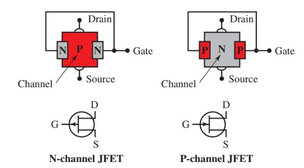
Figure 1. The physical construction of typical JFETs and their schematic symbols.
The current through the device is controlled by the gate potential. See Figure 2. If a small potential is applied to the gate, a large current through the P channel will exist.
If a large potential is applied to the gate, a small current will exist in the channel between the source and the drain. Notice how the potential applied at the gate pinches off the flow of electrical energy.
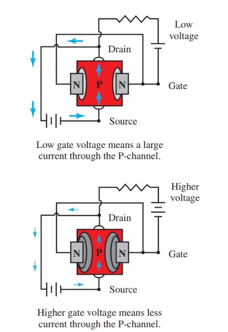
Figure 2. The amount of voltage applied to the gate will determine the current value from the source to the drain.
MOSFET Construction
Another type of FET is the MOSFET. It is used extensively in digital circuits and memory circuits in computers. Look at Figure 3.
The MOSFET is similar in construction to the JFET. The difference is that the MOSFET has a very thin film of insulation (silicon dioxide) between the gate and the channel area.
Caution
The layer of insulation is so thin that it can easily be damaged by static electricity. Care must be taken when handling MOSFET transistors and devices.
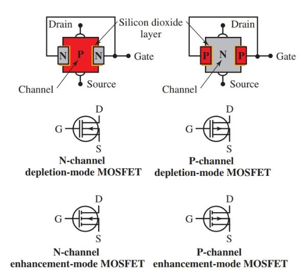
Figure 3. The MOSFET is similar in construction to the JFET.
The thin layer of high resistance insulation prevents electron flow between the gate and the channel material.
The high resistance between the gate and channel area makes for a very high impedance input device. A high impedance input device is very desirable in circuits such as amplifiers.
Also, the channel consisting of the same material from the source to the drain provides a very low impedance path. A low impedance, or low resistance, a path through the channel is also very desirable for devices such as amplifiers.
There are two main types of MOSFET, enhancement mode and depletion mode.
In a depletion-mode MOSFET, a current through the source-drain circuit is reduced by the gate voltage.
In an enhancement-mode MOSFET, a current through the source-drain circuit is increased by the gate voltage.
Look closely at the four symbols used for the MOSFET, Figure 3. The symbols differ for N-type and P-type channel materials and for enhancement-mode and depletion-mode MOSFETs.