The article provides an overview of the 741 operational amplifier, covering its basic characteristics, applications, and internal pin configuration. It also explains concepts like offset null, gain calculation, and comparator mode, highlighting its versatility in electronic circuits.
One of the most commonly used integrated circuit chips today is the operational amplifier. The operational amplifier is often simply called the op-amp.
741 Operational Amplifier Characteristics
- The 741 op-amp is a near-perfect amplifier.
- It has a high input impedance and a low output impedance, which makes it an excellent amplifier.
- The op-amp has a wide frequency response. This means the frequency of the signal being amplified has little effect on the operation of the amplifier as compared to other amplifiers.
- It has a high gain capability and can be adjusted for zero offset voltage. Having a zero offset voltage means it has features that allow the amplifier output to be adjusted to absolute zero voltage.
741 Operational Amplifier Applications
Many amplifiers have a slight output voltage due to temperature changes in the components. The op-amp can be corrected easily to compensate for temperature changes.
The 741 op-amp is a general purpose amplifier. It can be used to regulate power supplies, made into a simple signal generator, used as an oscillator, used as a radio or TV receiver, used as a timer, or used as a filter. It is also used extensively for instrumentation (metering current or voltage).
Originally, the term operational amplifier applied to any complete circuit designed from many discrete components that resulted in a high gain, high-performance dc amplifier. It was only natural that an amplifier used so extensively be designed as a single chip.
There are over twenty transistors in an op-amp chip along with all the resistors needed for bias. Using the op-amp IC saves time and money and also makes the repair and troubleshooting much simpler.
Op-amps need only a few exterior components such as resistors and capacitors to create an amplifier or one of many other devices.
Operation Amplifier Pin Configuration | Pin Layout
Figure 1 is an illustration of the pin configuration of a typical 741 general purpose op-amp. Like most IC chips, the op-amp does not have pin identification markings on the chip.
The pins are identified by using specifications sheets and a reference point. The reference point for our chip is the notch at the top. The pins are numbered in a counterclockwise direction, starting at the notch.
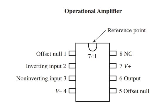
Figure 1. Pin identification of a typical dual-in-line package (dip) operational amplifier.
- The power for the op-amp is provided through pins 4 and 7.
- Pin 4 is either connected to ground or a negative voltage value from 3 to 18 volts.
- Pin 7 is connected to the positive voltage of the power supply.
- The output of the amplifier is pin 6.
- There are two input pins, pin 2 and pin 3. Pin 2 is the inverting input. Any signal applied to pin 2 generates a signal of opposite polarity at the output. The noninverting input, pin 3, generates an output at pin 6 of the same polarity. See Figure 2.
- Take special note that both inputs, pin 2 and pin 3, generate an output at pin 6, but they generate opposite polarities.
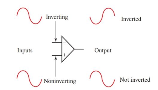
Figure 2. The polarity of the output signal of the op-amp is determined by the input signal location. The inverting input generates an output signal of opposite polarity to the input signal. The noninverting input produces a signal of matching polarity at the output.
741 Op Amp Offset Null
Offset null is a calibration feature of the op-amp. The op-amp is so sensitive to the input voltage that at times the output will generate a signal even when there is no intentional input. To avoid this condition for certain applications, offset null pins, pin 1 and pin 5 are provided. They are usually connected to a variable resistance such as a potentiometer. The potentiometer can be adjusted to produce a zero output voltage from pin 6.
Look at pin 8 and take note of the NC identification. This pin is not used. The NC stands for no connection.
Op Amp Gain
The op amp gain is easily determined by the relationship of the feedback resistor and the input resistor. Look at Figure 3. The feedback resistor is labeled RF and the input resistor is labeled RI.
To calculate the gain for the inverting op-amp in Figure 3 we simply divide the feedback resistor value RF (100 kΩ) by the input resistor value RI (10 kΩ). The gain (AV) for the op-amp is 10.
For a noninverting op-amp, the gain is equal to the feedback resistor value divided by the input resistor value plus one. The gain in the op-amp circuit shown would be 11. In the form of an equation:
AV (inverting) = RF ÷ RI
AV (noninverting) = (RF ÷ RI) + 1
Some op-amps can obtain a gain of 200,000 or higher.
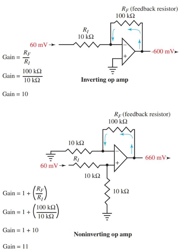
Figure 3. The gain is determined by the ratio of the input resistor to the feedback resistor value.
741 Op Amp Comparator Circuit
Another mode of operation of the op-amp is as a comparator circuit.
When operating as a comparator, both inverting and noninverting inputs are used. As the name comparator implies, the two inputs are compared to each other. The output of the comparator is driven to maximum positive or negative, depending on which input is more dominant.
Look at Figure 4. The comparator circuit is designed as a motor control system.
- It brings a dc motor up to running rpm and then maintains it. One input is wired to a potentiometer, while the other is connected to a small generator on the dc motor shaft.
- As the motor turns, a dc voltage is generated. The op-amp will continue to put out an inverted signal until the two inputs have a matching voltage amplitude.
- When the motor rpm is generating a slightly higher emf than the other input, the op amp switches to maximum opposite polarity.
- The op-amp changes output condition to match the input conditions. This output switching occurs so rapidly that it maintains motor rpm under changing mechanical load conditions.

Figure 4. The comparator mode of operation can be used as a motor control system. The output of the op-amp swings from and to maximum positive or negative polarity, depending on which input signal is greater.
Op-amps come in various forms. There can be more than one op-amp constructed on a single chip that takes the place of a multistage amplifier. They can be constructed from standard bipolar transistor construction or from MOSFET or JFET systems. The construction of an op-amp is determined by the electrical characteristics desired.
741 Operational Amplifier Key Takeaways
The 741 operational amplifier plays a vital role in modern electronics due to its remarkable characteristics and adaptability. Its high input impedance, low output impedance, wide frequency response, and adjustable gain make it a versatile component for countless applications. From regulating power supplies and generating signals to acting as comparators and filters, the 741 op-amp simplifies circuit design and enhances performance. Its internal configuration, including features like offset null and straightforward gain adjustment, allows for precise control in sensitive systems. These capabilities make the 741 op-amp essential in practical applications such as motor control, instrumentation, and signal processing, underlining its importance in both educational and industrial electronics.