The scientists John Bardeen and Walter Brattain invented the point-contact transistor. It had two wires carefully fused on a crystal of germanium. William Shockley followed these inventions by creating the bipolar, or junction, transistor. These inventions were the beginning of microelectronics.
The transistor provided instant circuit operation and eliminated the warm-up time needed with the vacuum tube circuit.
In addition, no large amounts of power were needed with the transistor. The transistor was and still is, known for its small size, long life, and lightweight.
Transistors are key devices in electronics for several reasons:
- They are able to amplify current.
- They can create ac signals at desired frequencies.
- They can also be used as switching devices. This makes them important in computer circuits.
The bipolar junction transistor (BJT) consists of three layers of impure semiconductor crystals. This transistor has two junctions. There are two types of bipolar transistors, NPN and PNP. Blocks and schematic symbols for these are shown in Figure 1.
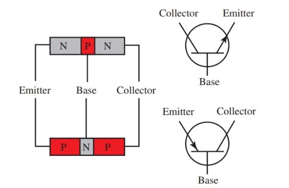
Figure 1. Block diagrams and symbols for NPN and PNP transistors.
The NPN bipolar transistor has a thin layer of P-type crystal placed between two N-type crystals, Figure 2a. A PNP bipolar transistor has a thin layer of N-type crystals placed between two P-type crystals, Figure 2b.
In both types, the first crystal is called the emitter. The center section is called the base. The third crystal is called the collector.
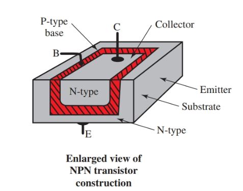
Figure 2a. NPN transistor.
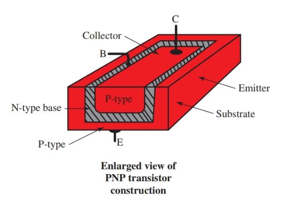
Figure 2b. NPN transistor.
NPN & PNP Transistor Symbols
In the schematic symbols in Figure 1, notice the direction of the arrow. This indicates whether it is an NPN or PNP transistor.
The arrow always points toward an N-type material. This will assist you in determining the proper polarity when making a connection in a circuit. The direction in which the emitter arrow points for an NPN transistor can easily be recalled by reciting “Never Points iN.”
Transistor Biasing
Figure 3 shows biasing diagrams for five transistors. Take special note of the fact that the base is not always the same pin location on the transistors. Never assume the proper connections. Always be sure by first checking the transistor part number in a catalog or product specification sheet.
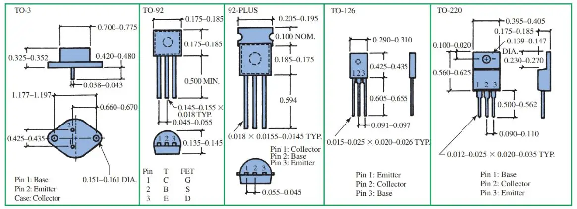
Figure 3. Biasing diagrams for five transistors. (DIGI-KEY)
NPN Transistor Working
The theory of NPN transistor working is shown in Figure 4.
- Two batteries are used to simplify operation theory. Most applications require one voltage source. The negative terminal of the battery is connected to the N emitter.
- The positive terminal of the same battery is connected to the P-type base. Therefore, the emitter-base circuit is forward biased.
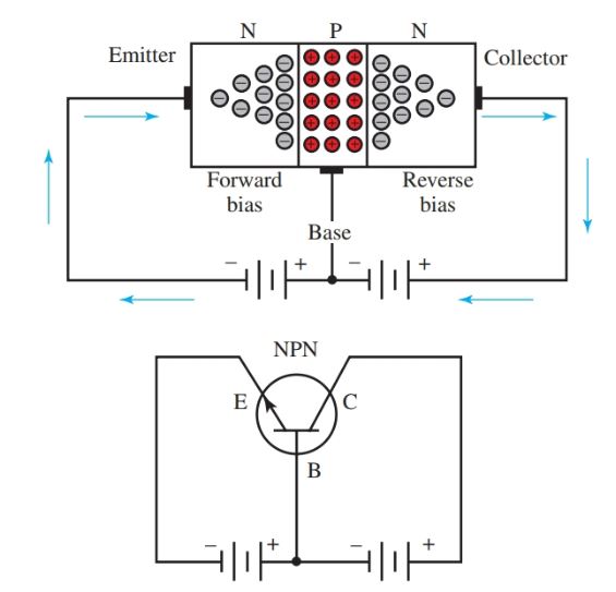
Figure 4. Current in an NPN transistor
- In the collector circuit, the N collector is connected to the positive battery terminal. The P base is connected to the negative terminal.
- The collector-base circuit is reverse biased.
- Electrons enter the emitter from the negative battery source and flow toward the junction. The forward bias has reduced the potential barrier of the first junction.
- The electrons then combine with the hole carriers in the base to complete the emitter-base circuit. However, the base is a very thin section, about 0.001 inches.
- Most of the electrons flow on through to the collector. This electron flow is aided by the low potential barrier of the second PN junction.
Approximately 95 to 98 percent of the current through the transistor is from an emitter to collector. About two to five percent of the current moves between emitter and base.
A small change in emitter to base bias voltage causes a somewhat larger change in emitter-collector current. This is what allows transistors to be used as amplifiers. The emitter-base current change, however, is quite small.
PNP Transistor
A PNP transistor has a P-type material for the emitter, an N-type material for the base, and a P-type material for the collector. See Figure 5.
The power supply or battery must be connected in the opposite way as an NPN transistor. Like the NPN transistor, the emitter-to-base circuit has a forward bias, and the collector-to-base circuit has a reverse bias. In a PNP transistor, most carriers in the emitter-to-collector are holes.
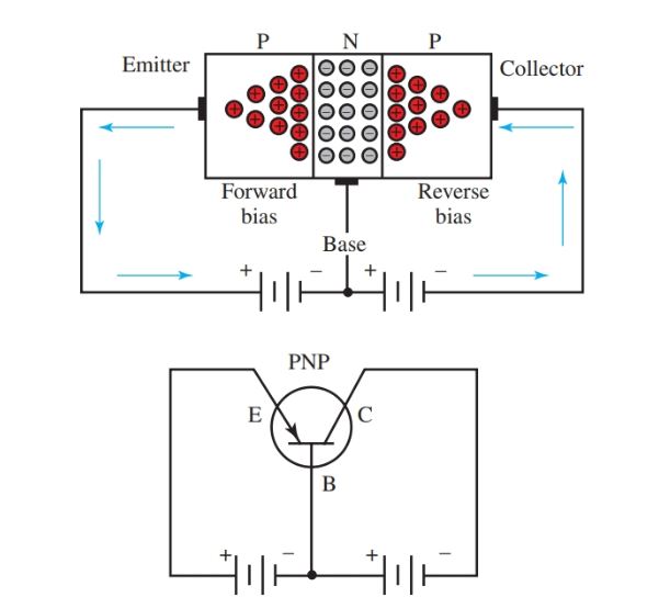
Figure 5. Current in a PNP transistor.