This article provides an overview of vertical metal-oxide semiconductor field-effect transistors (V-MOSFET), focusing on their structure, operation, and characteristic curves.
V-MOSFETs, or vertical metal-oxide semiconductor field-effect transistors, are an advanced form of field-effect transistors (FETs) developed for solid-state electronic applications. Designed to overcome the limitations of conventional transistors, V-MOSFETs offer superior performance in high-speed switching and power amplification. Their vertical structure allows for efficient current flow and enhanced thermal dissipation, enabling them to handle higher power levels with greater reliability. As a result, V-MOSFETs have become key components in modern power supplies, control systems, and other high-performance electronic circuits, often replacing traditional bipolar power transistors.
V-MOSFET Structure
The V designation refers to vertical-groove MOS technology. This device has a V-shaped groove etched into the substrate. Construction of this type requires less area than a horizontally assembled device. The geometry of a V-MOSFET device also permits greater heat dissipation and high-density channel areas. V-MOSFETs have fast switching speeds and lower channel resistance.
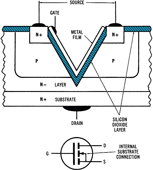
Figure 1. A cross-sectional view of an N-channel V-MOSFET with schematic symbol.
Figure 1 shows a cross-sectional view of the crystal structure, element names, and schematic symbol of an N-channel V-MOSFET. Note that a V-groove is etched in the surface of the structure. From the top, the V-cut penetrates through N+, P, and N− layers and stops near the N+ substrate. The two N+ layers are heavily doped, and the N− layer is lightly doped. A thin layer of silicon dioxide covers both the horizontal surface and the V-groove. The source leads on each side of the groove are connected internally. The bottom layer of N− material serves as a combined substrate and drain. Current carriers move between the source and drain vertically.
V-MOSFET Operation
A V-MOSFET responds as an E-MOSFET. No current carriers exist in the source and drain regions until the gate is energized. An N-channel device, such as the one in Figure 1, does not conduct until the gate is made positive with respect to the source. When this occurs, an N channel is induced between the two N+ areas near the groove. Current carriers can then flow through the vertical channel from source to drain. When the gate of an N-channel device is made negative, no channel exists, and the current carriers cease to flow.
P-channel V-MOSFETs are also available for use in electronic circuit applications. The current carriers of a P-channel device are holes. In general, holes are less mobile than electrons. These devices do not respond as well to high-frequency AC. The primary characteristics and theory of operation are, however, very similar to those of an N-channel V-MOSFET. Differences exist only in voltage polarity and current-carrier flow. As a rule, a wider variety of N-channel devices are manufactured because industrial applications tend to favor the N-channel devices over the P-channel devices.
V-MOSFET Characteristic Curves
The characteristic curves of a V-MOSFET are very similar to those of an E-MOSFET. Figure 2 shows the drain family of characteristic curves and the dynamic transfer curve of an N-channel V-MOSFET. This particular device is a power V-MOSFET.
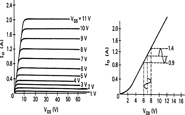
Figure 2. A drain family of characteristic curves and a transfer curve for an N-channel V-MOSFET.
Figure 2(a) shows that $V_{GS}$ must be positive with respect to the source if there is to be an increase in $I_{D}$. The value of $V_{GS}$ also controls $I_{D}$ for an increase in $V_{DS}$. Note that V-MOSFETs have ohmic and pinch-off regions very similar to those of an E-MOSFET.
In Figure 2(b), the dynamic transfer curve of V-MOSFET plots $V_{GS}$ and $I_{D}$ for a single $V_{DS}$ value. A change in $V_{GS}$ is considered to be a variation in the input voltage. $I_{D}$ is used to denote an output condition. A transfer curve shows how the output responds to a change in input voltage. This curve is nearly linear over its entire length. The forward transconductance ($g_{m}$) can be obtained from the data of this curve.
To determine the forward transconductance of a V-MOSFET, refer to Figure 2(b). In this case, the dynamic transfer curve shows an input voltage change of 2 Vpp with an operating point of 7 $V_{GS}$. A 2-Vpp input signal causes the operating point to change from 6 to 8 V. The resulting $I_{D}$ values are from 0.9 to 1.4 A. This represents a $\Delta I_{D}$ of 0.5 A. The $g_{m}$ is determined to be:
$$g_{m} = \frac{\Delta I_{D}}{\Delta V_{GS}} = \frac{(1.4 – 0.9)}{(8 – 6)} = \frac{0.5}{2} = 0.25S \quad or \quad 250 mS$$
Note that the $g_{m}$ of a V-MOSFET is quite large. Compared with other FETs, this is a very significant condition of operation. The voltage gain ($A_{V}$) of an FET amplifier is based on $g_{m} \times R_{L}$. With high values of $g_{m}$, it is possible to achieve a great deal; more voltage gain with a V-MOSFET than with other types of FETs. This feature, its power-handling capability, and high switching speed make the V-MOSFET an extremely attractive amplitude-control device for electronic circuits.
Review Questions
- The V in V-MOSFET stands for ________ groove MOS technology.
- V-MOSFETs are widely used in ________ and solid-state switching applications.
- The source and drain in a V-MOSFET are aligned ________.
- An N-channel V-MOSFET requires a ________ gate voltage to conduct.
- The forward transconductance of a V-MOSFET is represented by the symbol ________.
- In a dynamic transfer curve, the input voltage is represented by ________ and the output by ________.
- V-MOSFETs have ________ and pinch-off regions similar to E-MOSFETs.
- The voltage gain of an FET amplifier is calculated using the formula ________.
Answers
- vertical
- power supplies
- vertically
- positive
- $g_{m}$
- $V_{GS}$, $I_{D}$
- ohmic
- $A_{V} = g_{m} \times R_{L}$
Key Takeaways
V-MOSFETs combine compact vertical construction with high efficiency and fast switching capabilities, making them well-suited for power amplification and electronic switching. Their high transconductance and superior thermal management give them a performance edge in industrial and consumer electronics.