This article explores the structure, operation modes, and characteristic curves of Depletion-type MOSFETs (D-MOSFET), focusing on N-channel and P-channel variations and their application relevance.
Before diving into D-MOSFETs, it’s important to understand how they differ from E-MOSFETs (Enhancement-type MOSFETs). While E-MOSFETs are normally-off devices and operate only in enhancement mode, D-MOSFETs are normally-on devices that support both depletion and enhancement modes of operation. This distinction significantly affects how each device is biased and used in circuits.
D-MOSFET Structure
A depletion metal-oxide semiconductor field-effect transistor (D-MOSFET) has an interconnecting channel built into the substrate. The source and drain are directly connected by the channel. Channel construction of this device is very similar to that of a JFET. The MOSFET responds to the depletion of current carriers that pass through its channel.
Figure 1 shows a cross-sectional view of the crystal structure, element names, and symbols of a P-channel and N-channel D-MOSFET. In the N-channel device shown, a channel of N-type material is formed on a P substrate. The source and drain are connected by this channel. A thin layer of silicon dioxide ($SiO_{2}$) insulates the gate from the channel. The gate is simply a strip of metal that has been deposited on the $SiO_{2}$ layer. The entire assembly is built on a P substrate.
The schematic symbol of the device shows the source, substrate, and drain commonly connected together. This indicates that the source and drain are connected by a piece of channel material that is formed on a piece of substrate material. The substrate of the symbol is represented by an arrow. When the arrow points in toward the channel, it indicates that the substrate is P and the channel is N. The current carriers of an N-channel device are electrons.
P-channel device construction is similar to that of the N-channel device. The crystal material of the channel and substrate are of a different polarity. In a P-channel device, the current carriers are holes. The schematic symbol shows that the source, drain, and substrate are commonly connected. The substrate arrow does not point toward the channel. This indicates that the substrate is N-type material, and the channel is P-type material.
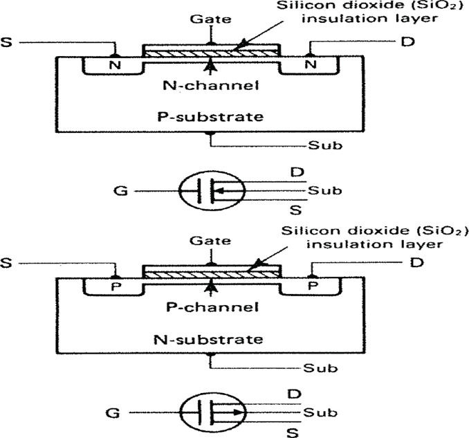
Figure 1. Crystal structures, element names, and schematic symbols of D-MOSFETs. (a) N-channel D-MOSFET. (b) P-channel D-MOSFET.
D-MOSFET Operation
The operation of a D-MOSFET is quite unusual compared with other FETs. With voltage applied to the source and drain only, drain current flows through the channel. In this condition of operation, the gate does not need voltage to produce conduction. A D-MOSFET, therefore, is classified as a normally-on device. Channel current ($I_{D}$), however, is controlled by different values of gate voltage. When the channel and gate voltages are of the same polarity, there is a reduction or depletion of current carriers. This condition of operation increases the channel’s depletion region. Depleting the number of current carriers in the channel causes a corresponding reduction in $I_{D}$. The depletion mode of operation represents only one form of control that can be achieved.
If the gate and channel of a D-MOSFET have a different polarity, the number of channel current carriers increases. This means that the device is capable of both depletion and enhancement modes of operation. Making the gate positive in an N-channel device increases the number of current carriers. In effect, this pulls electrons into the channel from the substrate. A negative gate voltage depletes the number of current carriers. This action increases the depletion region of the channel, which reduces $I_{D}$. A zero $V_{GS}$ divides the depletion and enhancement modes of operation. In a strict sense, this device could be called an enhancement-depletion MOSFET.
D-MOSFET Characteristic Curves
A drain family of characteristic curves for an N-channel D-MOSFET is shown in Figure 2. A family of curves for a P-channel D-MOSFET would be the same, except that the top $V_{GS}$ lines would be negative values and the gate polarity would be opposite. Note, in this display, that 0 $V_{GS}$ is near the center of the curves. This divides the enhancement and depletion modes of operation. For AC amplification, an ideal operating point is 0 $V_{GS}$. For the N-channel display, the positive alternation of an input signal causes an increase in $I_{D}$. The negative alternation produces a decrease in $I_{D}$.
P-channel D-MOSFETs are not as readily available as N-channel devices because P-channel devices are somewhat more difficult to fabricate than N-channel devices and, in general, are more costly to produce. Most applications tend to favor the N-channel D-MOSFET. N-channel devices have better current mobility. This is a desirable feature in high-frequency AC signal amplification, where these devices are widely used.
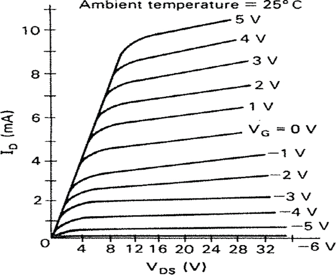
Figure 2. A drain family of characteristic curves for an N-channel D-MOSFET.
Review Questions
- In a D-MOSFET, the ______ connects the source and drain.
- The insulating layer between the gate and the channel is made of ______.
- The current carriers in an N-channel D-MOSFET are ______.
- When $V_{GS}$ is zero, the D-MOSFET operates at the ______ point for AC amplification.
- A D-MOSFET is considered a ______ device because it conducts with zero gate voltage.
- Applying a negative voltage to the gate in an N-channel D-MOSFET ______ the number of current carriers.
- The symbol arrow points toward the channel in a ______ substrate device.
- In enhancement mode, making the gate voltage positive in an N-channel device will ______ the drain current.
- P-channel D-MOSFETs are less common because they are more ______ to produce.
- The two modes of operation in a D-MOSFET are ______ and ______.
Answers
- channel
- silicon dioxide ($SiO_{2}$)
- electrons
- midpoint or ideal
- normally-on
- reduces
- P-type
- increase
- difficult
- depletion, enhancement
Key Takeaways
D-MOSFETs are unique semiconductor devices that can operate in both depletion and enhancement modes, making them highly versatile for analog and switching applications. Their normally-on behavior, ability to function without gate bias, and efficient current modulation allow for robust use in AC amplification and high-frequency systems.