This article discusses how transistor amplify electrical signals, focusing on their ability to increase voltage and current, with examples illustrating a common-emitter configuration for voltage amplification and the role of circuit components like capacitors and resistors in shaping the signal output.
A transistor functions as an amplifier by increasing the strength of a weak electrical signal. In an amplifier configuration, such as the common-emitter design, a small input signal applied to the base is converted into a larger output signal at the collector. This amplification occurs due to the transistor’s ability to control a large collector current using a much smaller base current, with the gain depending on the transistor’s configuration and circuit design.
There are three main transistor configurations for amplification: common-emitter (CE), common-base (CB), and common-collector (CC). The CE configuration is the most commonly used, offering high voltage and current gain, while the CB configuration provides high voltage gain with low input impedance, suitable for high-frequency applications. The CC configuration, known for its high current gain and low output impedance, is ideal for impedance matching.
Amplifiers can operate in various classes based on efficiency and linearity, including Class A, B, AB, and C. Class A amplifiers provide high linearity with low distortion but are less efficient, while Class B and AB amplifiers improve efficiency with some distortion, making them popular in audio applications. Class C amplifiers are highly efficient and suitable for RF and high-frequency operations.
Key parameters influencing a transistor’s amplification include gain (β or hFE), which determines the amplification capability, input and output impedance, affecting signal compatibility and efficiency, and frequency response, indicating the range of frequencies an amplifier can handle effectively. Proper biasing is crucial for maintaining the transistor in its active region, ensuring linear amplification, while techniques like using feedback resistors enhance stability and prevent issues like thermal runaway.
Capacitor coupling is often employed to block unwanted DC components and ensure clean signal amplification, while the phase relationship in a common-emitter configuration introduces a 180° phase shift between input and output signals. Understanding these aspects allows transistors to be effectively utilized in a wide range of electronic applications, from amplifying audio signals to processing data from sensors.
Voltage Amplification Example
The circuit in Figure 1 illustrates a simple example of how the voltage of a simple sinusoidal signal can be amplified. In other words, if a sinusoidal signal is introduced as the input of a transistor, the transistor output is a similar signal (having the same form and frequency) with a higher voltage. We study the variation of the voltage across the load and compare it with the input voltage.
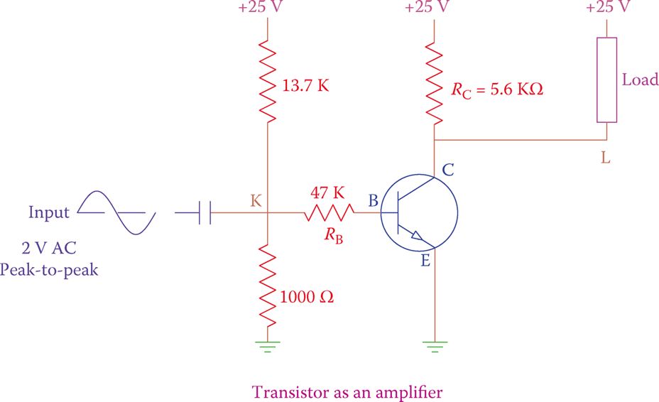
Figure 1. Voltage amplification by a transistor circuit diagram
The input is a sinusoidal voltage with a peak-to-peak value of 2 V introduced at point K, which is connected to the transistor base through a 470 kΩ resistor. The other wire for this signal is connected to the ground.
The role of the capacitor before point K is very important. It filters (prevents from passing) any DC content that may be blended with the input signal.
The corresponding values for the input (the sinusoidal waveform) and the output (voltage across the load) for each 30° of the one cycle are entered in Table 1, together with some other values, as discussed.
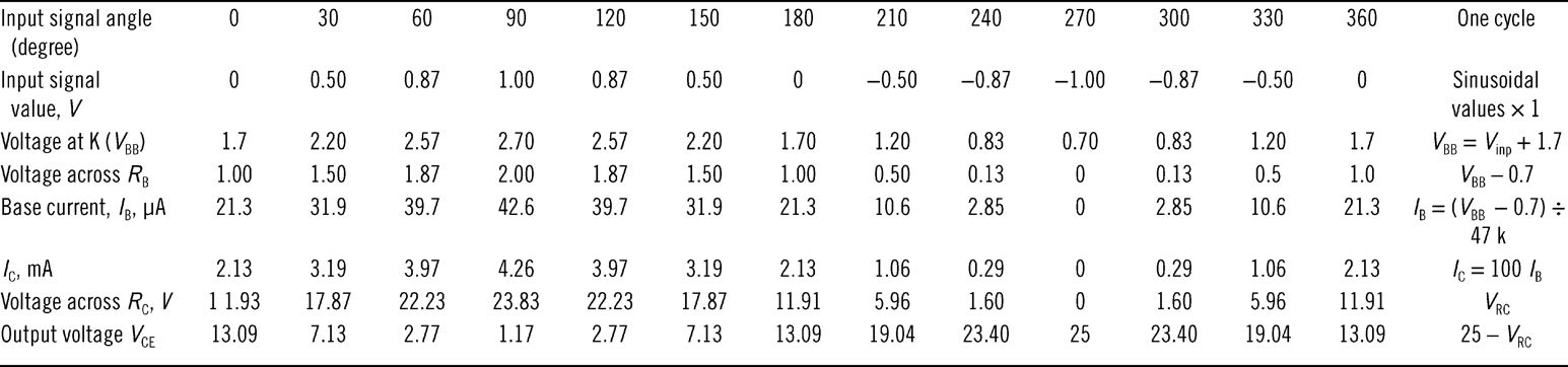
TABLE 1 Variation of Input versus Output Voltage for the Circuit of Figure 1
Assuming that this transistor is made out of silicon because in a silicon base transistor there is always a voltage drop of about 0.7 V between the base and the emitter, the voltage at K must be such that it never goes below 0.7 V. Otherwise, the transistor goes to cutoff state and stops conducting.
In this example, the 13.7 kΩ and 1000 Ω resistors form a voltage divider to provide 1.7 V DC at point K. This value of 1.7 V has been specifically selected such that for the most negative value of the sinusoidal wave the base-emitter junction is still forward biased and its VBE is not less than 0.7 V (1.7 − 1/2 × 2) = 0.7 V; the input is 2 V peak to peak.
The 2 V peak-to-peak value AC signal and the 1.7 V DC signal add together and, as a result, the voltage at point K has a variation between 2.7 and 0.7 V.
Table 1 shows the following values for 12 different points (360° at 30° intervals):
- Input signal angle at various instants during one cycle.
- Input signal voltage.
- The voltage at point K.
- VBE(Voltage at K − 0.7 V).
- Base current, in microampere (μA), based on Ohm’s law VBE/470 kΩ.
- Collector current in mA, assuming 100× the base current (IC = βIB= 100IB).
- Voltage drop in resistor R (see Figure 1).
- The voltage at point L. This is VCE, because the emitter is grounded, VCE= 25 V – voltage drop in the 5.6 kΩ resistors.
Notice that here we have intentionally connected the load across the 5.6 kΩ resistors. The variation of the voltage across the load is sinusoidal, that is, similar to the input. Although this way of connecting the load is possible, it is not the only way to do so.
The load could be connected between the ground and point L. For this configuration, both the output voltage and the voltage across the load have sinusoidal forms, but the two voltages have a 180° phase difference.
Figure 2 shows the relationship between the voltages of the input and output signals (rows 2 and 8 of Table 1). There are a number of important points that can be observed from Figures 1 and 2:
- The transistor is used in a common-emitter configuration.
- The input signal has a sinusoidal waveform.
- The input signal was blended with a positive DC value to create a varying DC (varying in value, but otherwise always positive) signal.
- The output is also always positive, but it has a variation in the form of a sinusoidal wave.
- The output variation (sinusoidal pattern) has the same frequency as the input.
- The peak to peak of the output voltage variation has a larger value than that of the input signal.
- When the input signal is at its maximum, the output signal is at its minimum, and vice versa. That is, the output is 180° out of phase with the input.
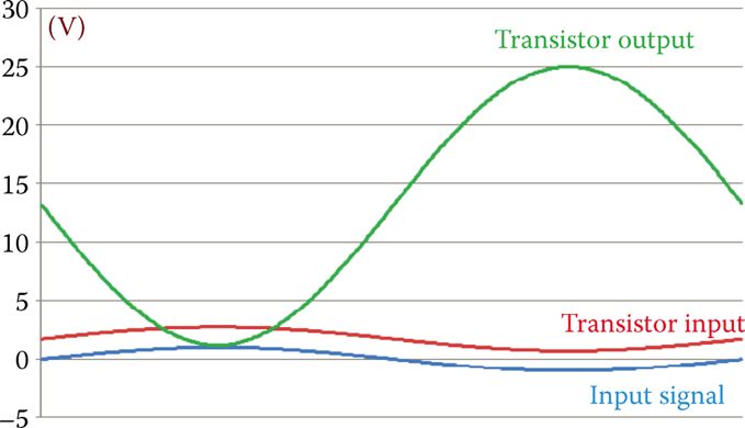
Figure 2 Input and output relationship in a transistor when used in common emitter design.
In the same way that the input signal was blended with a constant DC voltage, the output signal has a DC content, as seen in Figure 2.
To remove the DC content of the output signal, a capacitor is added to the circuit at a point where the output signal is taken (point L).
The revised circuit is as shown in Figure 3. This capacitor of appropriate value can filter out the DC content (block the DC current). The outcome of this filtration is a signal that varies between −11.9 and +11.9 V, $\left( \frac{25-1.2}{2} \right)$, that is, its peak-to-peak value is about 23.8 V. Figure 4 depicts the voltages at points H, K, L, and M of the circuit in Figure 3; the ratio of amplification, however, is shown smaller in order fit the page.
The input signal is introduced between point H and the ground, and the output signal is taken between point M and the ground. The sinusoidal input signal was amplified by 11.9× (the ratio between the peak value of the output and the peak value of the input).
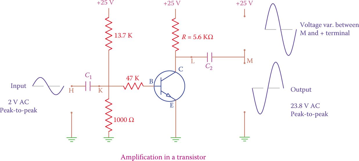
Figure 3 Capacitor C2 is added to the circuit in Figure 2.
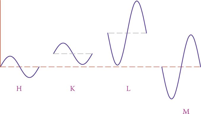
Figure 4 Voltage forms at various points of the circuit in Figure 3.
Transistor as an Amplifier Key Takeaways
Understanding how transistors amplify electrical signals—especially in configurations like the common-emitter design—is essential for their effective use in a wide range of real-world applications. These principles are critical in designing amplifiers for audio systems, communication devices, and sensor signal processing, where precise control of signal strength and integrity is required. Components such as resistors and capacitors, along with proper biasing and configuration, allow engineers to tailor transistor behavior for specific tasks, ensuring reliable and efficient performance.