The article provides an overview of basic logic gates used in electronic circuits, including their definitions, symbols, truth tables, and examples. It covers the operation and characteristics of gates such as AND, OR, NOT, NAND, NOR, XOR, and XNOR, highlighting how they form the foundation of digital logic systems.
Logic Gates
Electronic switching circuits that govern, or “decide,” whether inputs will pass to output or be stopped are called logic gates. The logic gates discussed here are the building blocks for other logic gates. The basic logic gates are:
- AND gates.
- OR gates.
- NOT gates.
- NAND gates.
- NOR gates.
- XOR gates.
- XNOR gates.
All logic gates can be made from some combination of the first three gates in the list, the AND, OR, and NOT gates.
AND Gates
The AND gate accepts high and low inputs (1 and 0). Based on these inputs, the gate decides on the output. The outputs of AND gates are also high or low. The AND gate symbol is shown in Figure 1.
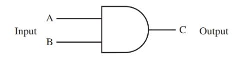
Figure 1. AND gate symbol.
The AND gate produce an output of 1 (high) if all inputs are 1 (high). Logic 1 or high also equal on. A simple circuit with switches that functions like an AND gate is shown in Figure 2. Both switches are off (0 or low). The lamp does not burn. When both switches are on, the lamp burns, Figure 3. If only one or the other gate is on, the lamp does not burn. This simple circuit using SPST switches illustrates AND gate operation, however, the actual AND gate used in a computer is very complex.
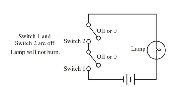
Figure 2. This simple switching circuit simulates the operation of an AND gate. The lamp will not burn because both switches are off.
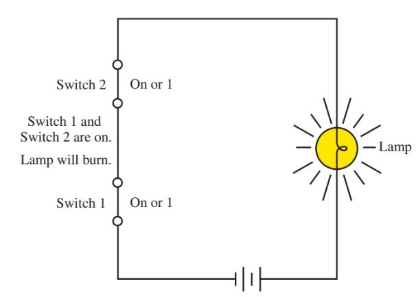
Figure 3. This is the same circuit as in Figure 2. However, the lamp will burn because both switches are on.
A binary table that explains the operation of the AND gate is shown in Figure 4. This table is called a truth table. The truth table shows the inputs on the left and outputs on the right.
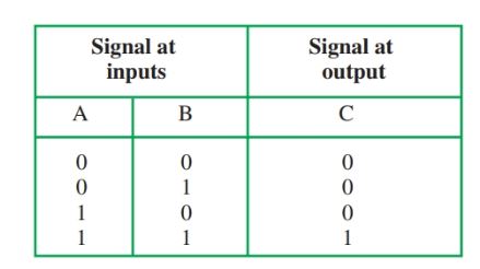
Figure 4. AND gate truth table. Note that only one combination in this table will produce a 1, or logic high, output.
The AND gate is used to detect the presence of high signals, or ls, on both inputs A and B. If this occurs, the output signal will be 1. However, if even one input signal is 0, the output will be 0. The output signal as affected by input signals in the AND gate is shown in Figure 5.

Figure 5. Resulting valid logic highs and lows in an AND gate as they appear on a three-channel oscilloscope.
OR Gates
The OR gate provides an output signal of 1 (high) when either one of its inputs or both of them is 1. If all inputs are 0 in an OR gate, the output is a 0 (low). The OR circuit detects the presence of any high input. The symbol for an OR gate is shown in Figure 6.
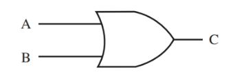
Figure 6. OR gate symbol.
The truth table for an OR gate is shown in Figure 7. The schematic for an OR gate created from switches is shown in Figure 8. The OR gate acts like two switches in parallel. The output signal, as it is affected by input signals in the OR gate, is shown in Figure 9.
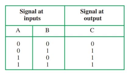
Figure 7. OR gate truth table.

Figure 8. Schematic of a simulated OR gate. The lamp will not burn in this instance.
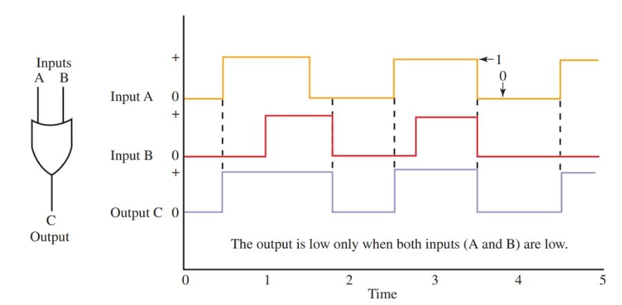 Figure 9. Valid logic highs and lows for OR gate.
NOT Gates
The NOT gate is put into a circuit to invert the polarity of the input signal. The NOT gate is often called an inverter because the name describes its function. If the input signal is 1, the output signal will be 0. Likewise, if the input signal is 0, the output will be 1.
The symbol for the NOT gate is shown in Figure 10. Note that the NOT gate symbol has only one input lead. Notice that there is also a small circle at the end of the triangle in the symbol.
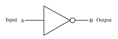
Figure 10. NOT gate symbol.
The schematic for a simulated NOT gate circuit is shown in Figure 11. The NOT gate truth table is shown in Figure 12. Figure 13 shows the output signal in a NOT gate as affected by the input signals.
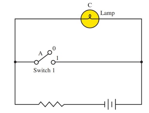
Figure 11. Schematic of simulated NOT gate. The input is 0, so the output is 1.
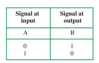
Figure 12. NOT gate truth table.
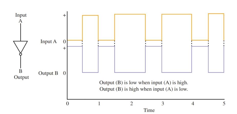
Figure 13. Valid logic highs and lows for NOT gate.
NAND Gates
All logic gates are combinations of the basic gates: AND, OR, and NOT. The NAND gate is a negative AND gate. It is made up of an AND gate and a NOT gate. It is also called a NOT AND gate.
The NAND gate symbol is like the AND gate symbol with a circle at the end, Figure 14. The schematic for a NAND gate circuit simulated from switches is shown in Figure 15. The NAND truth table is shown in Figure 16. Notice that this truth table is the reverse of the AND truth table. Figure 17 shows the waveforms in a NAND gate circuit.
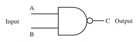
Figure 14. NAND gate symbol.

Figure 15. Schematic of a simulated NAND gate. The inputs are 0 and 0, so the output is 1.
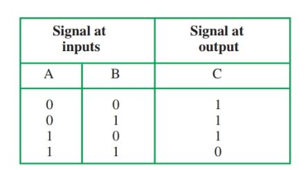
Figure 16. NAND gate truth table
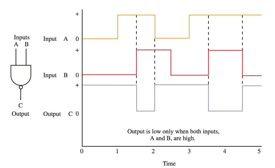
Figure 17. Valid logic highs and lows for NAND gate.
NOR Gates
The NOR gate gives the opposite (or negative) results of the OR gate. The NOR gate is made up of an OR gate and a NOT gate (inverter). The symbol for a NOR gate is shown in Figure 18. Figure 19 shows the schematic for a NOR circuit simulated with switches.
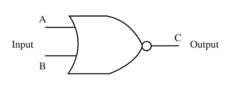
Figure 18. NOR gate symbol.
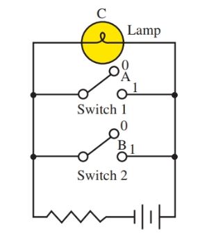
Figure 19. Schematic of simulated NOR gate. The inputs are 0 and 0, so the output is 1.
The NOR circuit is used to test for any kind of input. If there is no input, the output will be 1. If there is an input, the output will be 0. This is shown in the truth table in Figure 20. Notice that the truth table for the NOR gate is the exact opposite of the truth table for the OR gate. The waveforms of a NOR gate circuit are shown in Figure 21.
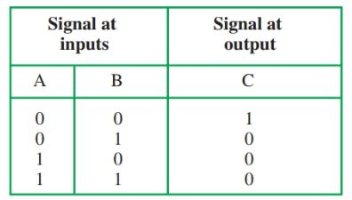
Figure 20. NOR gate truth table.
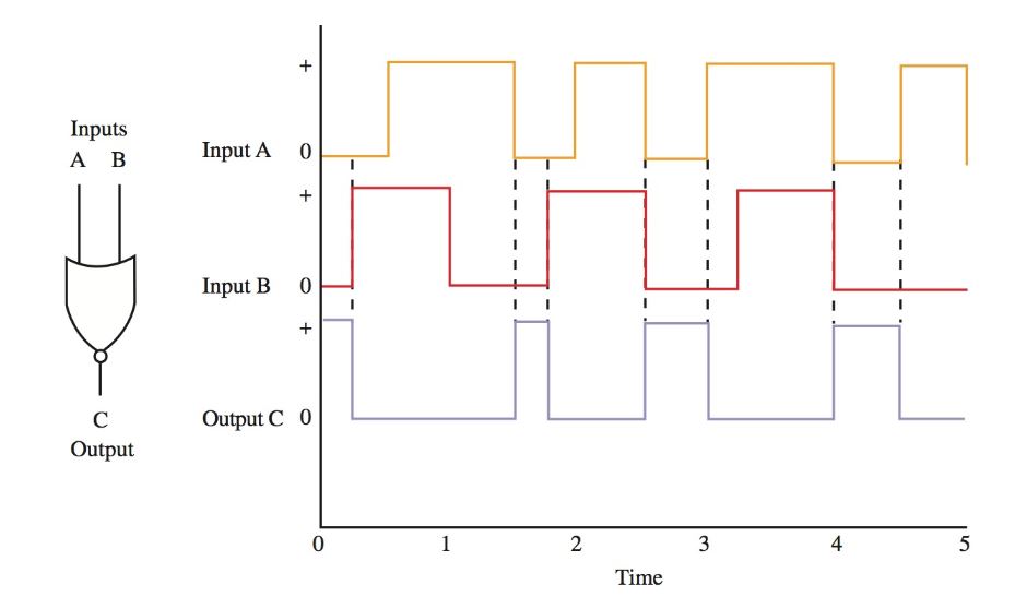
Figure 21. Valid logic highs and lows for NOR gate.
XOR Gates
There is a special type of gate that provides a high output whenever any, but not all, inputs are logic high. It is called the exclusive OR gate or the XOR gate. Recall that in contrast, the OR gate provides a high output whenever any or all inputs are logic high.
The symbol for the XOR gate is shown in Figure 22. The circuit that simulates the XOR gate using two single-pole, double-throw switches is shown in Figure 23. The XOR gate truth table is shown in Figure 24. The waveforms of an XOR gate circuit are shown in Figure 25.
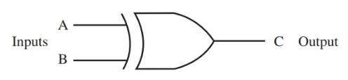
Figure 22. XOR gate symbol
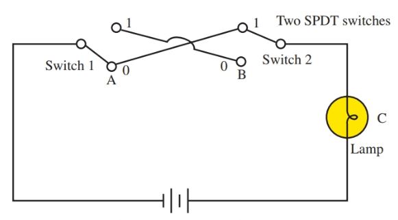
Figure 23. Schematic of simulated XOR gate. Note that it has two SPDT switches. One input is 1 and the other is 0. The output will be 1.
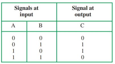
Figure 24. XOR gate truth table.
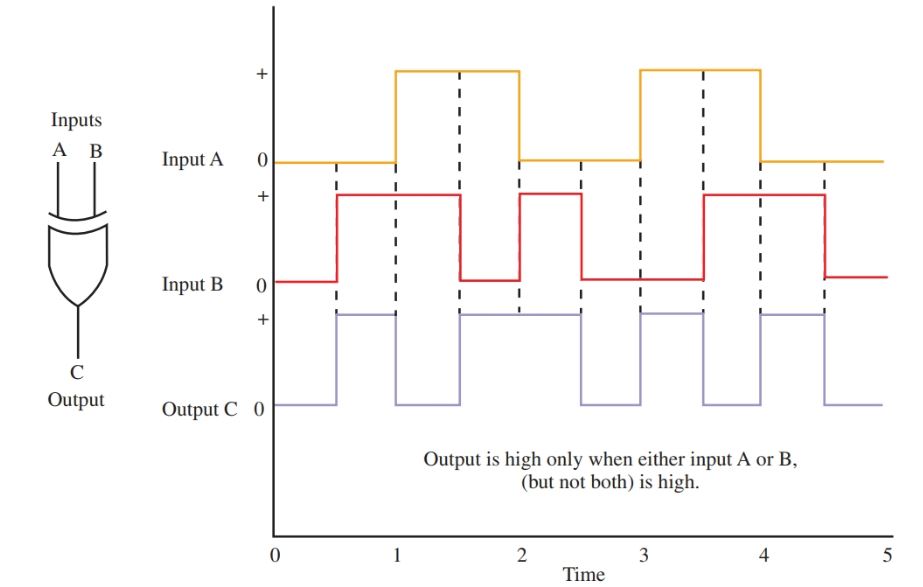
Figure 25. Valid logic highs and lows for XOR gate.
XNOR Gates
A gate similar to the XOR gate is the exclusive NOR gate, or XNOR gate. This gate is the XOR gate with the output inverted. There is a high output only if all inputs are logic high or logic low. The symbol for the XNOR gate is shown in Figure 26. The truth table is shown in Figure 27. Notice that if only one input is high (column A or column B), there is a zero in column C. If column A and column B both have a 0s or both have 1s, then column C has a 1.
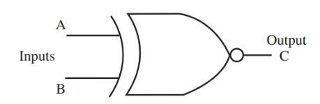
Figure 26. XNOR gate symbol.
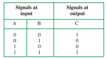
Figure 27. XNOR gate truth table.
Basic Logic Gates Key Takeaways
Understanding the function and behavior of basic logic gates—AND, OR, NOT, NAND, NOR, XOR, and XNOR—is essential because they serve as the foundation of all digital electronic systems. These gates are the building blocks of complex circuits used in computers, mobile devices, and various forms of automation. From performing arithmetic operations and storing data to controlling decision-making processes in microcontrollers, logic gates make it possible for digital systems to process and respond to inputs effectively.