The article provides an overview of transistor, including their basic structure and types, modes of operation, and the importance of proper biasing for their function. It also explains how transistors are used in circuits as amplifiers or switches and highlights their physical packaging and heat management.
A transistor is a semiconductor device with many applications. It is, in fact, the mother of all the other semiconductor electronic devices that we use or see around us today.
Before transistors were invented, all electronic devices were made with vacuum tubes. Still one can find devices such as stereo amplifiers and radio receivers that use vacuum tubes, but they are rare and expensive, in addition to being bulky and heavy in comparison to solid-state electronics that use transistors and semiconductor technology.
There are various types of transistors and the simplest form of the transistor is a junction transistor, also called bipolar junction transistor. The reason for calling it junction transistor is because it contains two PN junctions. In other words, from the structure viewpoint, it is similar to two diodes put together during the manufacturing process.
Nonetheless, note that a transistor is a completely different device than a diode, meaning that one cannot put two diodes together and expect to have a transistor.
Junction transistor: Same as bipolar junction transistor, which includes an ordinary transistor.
Bipolar junction transistor: Another name for junction transistor.
Junction Transistor
Recalling that a PN junction has a P side and an N side, imagine you want to put two of them together. It is easy to understand that depending on how they are put together, two basic types of transistors can result, as shown in Figure 1.
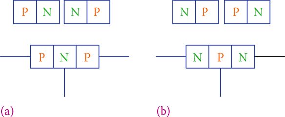
Figure 1 Two basic types of transistors: (a) PNP and (b) NPN.
Accordingly, the two types of a junction transistor are PNP and NPN. This classification is based on the polarity in the structure. There are other types of classification, based on transistor functioning and performance in a circuit.
As can be easily understood from Figure 1, a transistor has three terminals. In a transistor, irrespective of the type (PNP or NPN), the middle terminal is called the base. The other two terminals are called the emitter and the collector.
The internal structure of a transistor and the amount of doping in each P and N material (which determine the thickness of the depletion region in a PN junction) determine which side is the emitter and which is the collector.
The emitter junction is much higher doped than the collector junction. Figure 2 shows the symbols for junction transistors, where B, C, and E identify the base, emitter, and collector, respectively.
Base: One of the three principal terminals of a junction transistor (ordinary transistor).
Emitter: One of the three main terminals of a common (not FET) transistor.
Collector: One of the three main terminals of an ordinary transistor.
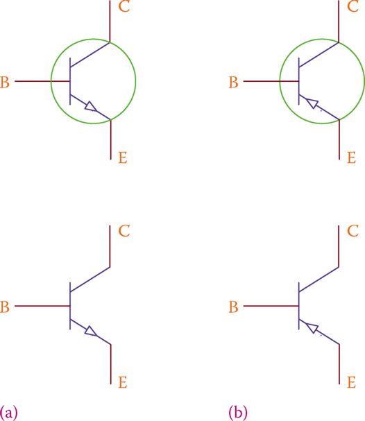
Figure 2 Symbols for (a) NPN transistor and (b) PNP transistor.
The emitter is identified by an arrow, which shows the direction of the current. Note the difference between the two symbols. The direction of the arrow in the two transistor types are from positive to negative, or better say from P to N, where P and N refer to the semiconductor material type.
Transistor Size and Packaging
Transistors come in various packages (their physical form), the most common of which are shown in Figure 3. Their size is comparable with paper clips, as shown in Figure 4.
Like any other device, a transistor has ratings for current, voltage, and power. These are defined in the data sheet of each transistor and must be respected when used in electrical and electronic circuits.

Figure 3 Examples of physical shape (packaging) of transistors.
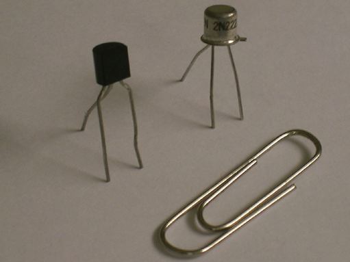
Figure 4 Indication of the size of a typical transistor.
Transistors may get hot when operating. In such a case a heat sink may be attached (screwed or glued) to its body. A heat sink is not part of a transistor; it is used for any component that can get hot in operation. It is a piece of metal (normally aluminum) with a large area (so that it can easily exchange heat with its surrounding environment), sometimes corrugated, which is attached to the body of a component that can get hot. This is a common practice, particularly in electronic devices.
A heat sink can be air cooled or in very high power devices can even be water cooled. Figure 5 shows a resistor with a large heat sink. Part of the reason for different packaging of transistors is the heat that they produce in operation. Only three of the transistors in Figure 3 can accept a heat sink.
Heat sink: Piece of aluminum attached to an electronic component to provide a larger area of contact with air, so that the heat produced in the component is removed from it better and faster and overheating and damage is prevented.
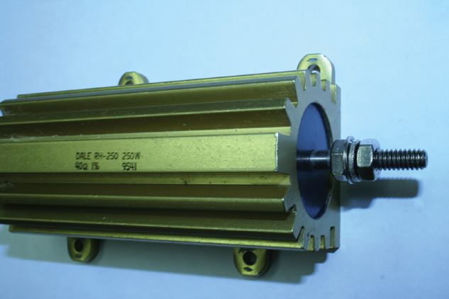
Figure 5 Example of a heat sink for a resistor.
For transistors with three in-line terminals (all three in a row; see Figure 3), usually, the connection in the middle is the base, and the other two could be marked or unmarked. But, this is not always the case. One must determine the base, emitter, and collector terminals before use.
Transistors Connection and Biasing Configuration
Because a transistor has three terminals, three different voltages can appear at each terminal when inside a circuit. In other words, on the basis of the currents in the circuit, the voltage at each terminal can be different than the other two.
The normal operating condition of a transistor requires that the junction between the collector and the base be reverse biased and the junction between the emitter and the base be forward biased. In this sense, the correct connections for a PNP and an NPN transistor are different. Two possible cases are shown in Figure 6a and b, for NPN and PNP transistors, respectively.
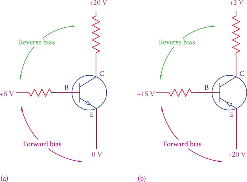
Figure 6 Correct connection of (a) NPN and (b) PNP transistors.
In the NPN transistor (see Figure 6a) the base is a P-type material and the collector is an N-type material. When the voltage at the collector terminal is larger than that at the base terminal, the collector-base junction is reverse biased. Also, in this transistor, the voltage at the B terminal is larger than the voltage at the E terminal. Thus, the base-emitter junction is forward biased.
Note that a 0 voltage means that the emitter is connected to the reference voltage, which can be the negative terminal of the DC power supply or the ground voltage.
Similarly, in Figure 6b the voltages at the B, E, and C terminals are +15, +20, and +2 V, respectively. This implies that the voltage at B (N side of the base-collector junction) is greater than the voltage at C terminal (thus, reverse bias) and the voltage at B is smaller than the voltage at E terminal (thus, forward bias).
For a transistor to function the condition is that (1) the emitter-base junction be forward biased and (2) the collector-base junction be reverse biased.
Modes of Operation
As we will learn gradually, most applications of a transistor are for switching and for amplification.
In switching, a transistor is used as a switch, meaning that it can turn on and off a device or part of a circuit. As for amplification, a transistor can be used as a voltage amplifier, a current amplifier, or a power amplifier.
In both switching and amplification, there is an input signal to the transistor and an output signal from the transistor. For each signal (input and output), two connections are necessary, as shown in Figure 7. This figure symbolizes a transistor as an input-output device, each one with an internal resistor between the two terminals.
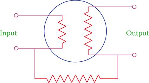
Figure 7 Input and output concept in a transistor.
When a signal is introduced to the input terminals, the corresponding output signal is generated and is available at the output terminals.
Because a transistor has only three physical terminals to the outside world, in order to have two input lines and two output lines, two of the terminals can be assumed to be internally connected, through an internal resistor. In other words, one of the terminals must be shared between the input and the output.
- You May Also Read: Transistor as an Amplifier: Working & Circuit | NPN Transistor Amplifier
In a circuit containing a transistor, in order that the correct biasing as mentioned above is respected, the transistor can be used in three different ways. These different ways are based on which terminal is shared between the input and output and define three modes of operation of transistors.
These three modes are common base, common emitter, and common collector. As the name implies, in each mode one of the terminals is common for both input and output.
Common base: One of the three configurations for using transistors in a circuit, where the base is a part of both the input and the output.
Common emitter: One of the three configurations for using transistors in a circuit, where the emitter is a part of both the transistor input and its output.
Common collector: One of the three configurations for using transistors in a circuit, where the collector is a part of both the transistor input and the output.
Figure 8 shows the three modes of operation for an NPN transistor. The same three modes are possible if a PNP transistor is used, but they are not shown here.
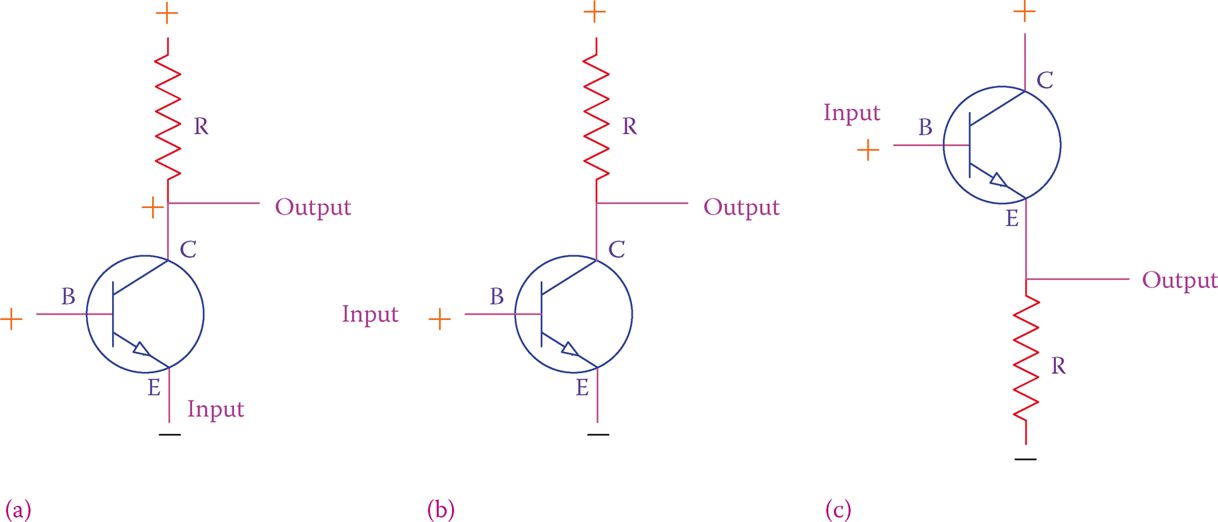
Figure 8 Three modes of operation of transistors: (a) common base, (b) common emitter, and (c) common collector.
In Figure 8a the input signal is introduced between the emitter and the base and the output is taken between the base and the collector.
The + and – signs showed are for the voltage, which must be such that the corresponding junctions have the correct bias.
It is obvious that the voltages and currents must be compatible so that the base can be connected to both the input circuit and the output circuit. The same principle applies to the common-emitter and common-collector configurations.
Later, we see that both correct biasing and voltage compatibility are achieved by having the appropriate resistors or other components in the circuits of each of the three terminals.
Transistor Key Takeaways
Transistors are fundamental components in modern electronics due to their versatility and efficiency. Their ability to function as both amplifiers and switches makes them essential in countless applications, from communication systems and computers to household appliances and medical devices. Unlike bulky and less reliable vacuum tubes, transistors offer compact size, lower power consumption, and greater reliability, enabling the miniaturization and performance improvement of modern electronic circuits.