Definition: An amplifier is an electronic circuit that uses a small input signal to control a larger output signal.
In electronics, amplifiers have been used since the early twentieth century. Amplification can be accomplished using vacuum tubes or semiconductor devices such as transistors or integrated circuits.
The amount of amplification in a circuit is known as gain. The gain is the ratio between the strength of the output (current, voltage, or wattage) and the strength of the input (current, voltage, or wattage), Figure 1.
Amplifier circuits can be thought of as control circuits. A small amount of current or voltage can control a larger amount of voltage or current. These circuits produce outputs that vary or are linear.
Amplifier devices such as transistors or ICs can also be used to switch current on or off, depending on how they are biased in the circuit.
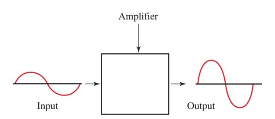
Figure 1. Block diagram of an amplifier.
Amplifier Biasing
For amplifiers to operate properly, they must be correctly biased.
Biasing means setting up the correct dc operating voltages between input leads of a transistor.
There are two junctions in a transistor. One junction is between the emitter and the base and is called the emitter junction. The other is between the collector and the base and is commonly referred to as the collector junction.
For proper transistor operation, energy from the internal power source (battery or power supply) is needed to overcome these junction resistances.
A bias voltage must exist between emitter and base of an NPN transistor, Figure 2. The voltage applied to these elements with the correct polarity will create current flow. This is known as forward bias. Reverse bias is needed in the collector junction of an NPN transistor, Figure 3.
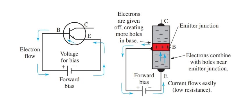
Figure 2. Forward bias for emitter junction in an NPN transistor.
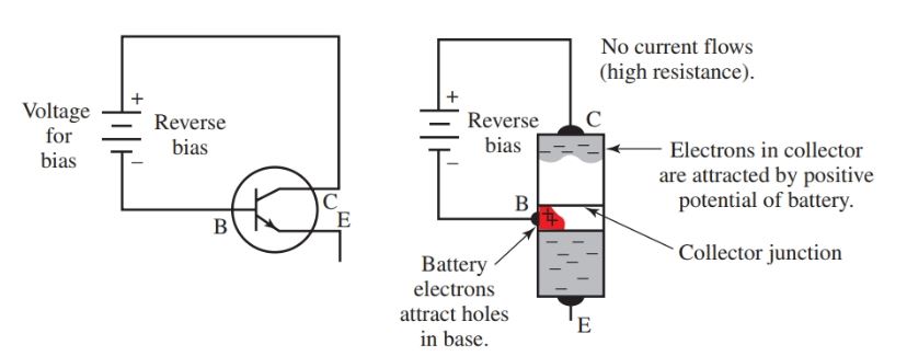
Figure 3. Reverse bias for collector junction in an NPN transistor
NPN Transistor Amplifier Working
Both forward and reverse bias are needed for the operation of a transistor amplifier. Figure 4 shows a complete NPN transistor circuit. Notice the forward bias in the emitter junction and reverse bias in the collector junction.
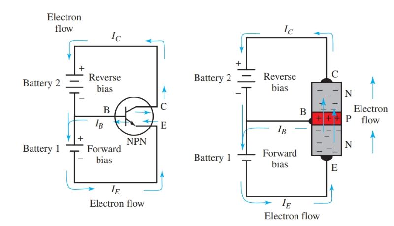
Figure 4. Forward and reverse bias in an NPN transistor amplifier circuit.
The same type of bias is needed for operation of a PNP transistor amplifier, Figure 5. The currents for each circuit are labeled. IE is for emitter current, IC for collector current, and IB for base current.
The emitter junction bias is provided by battery 1, and the collector junction bias is provided by battery 2.
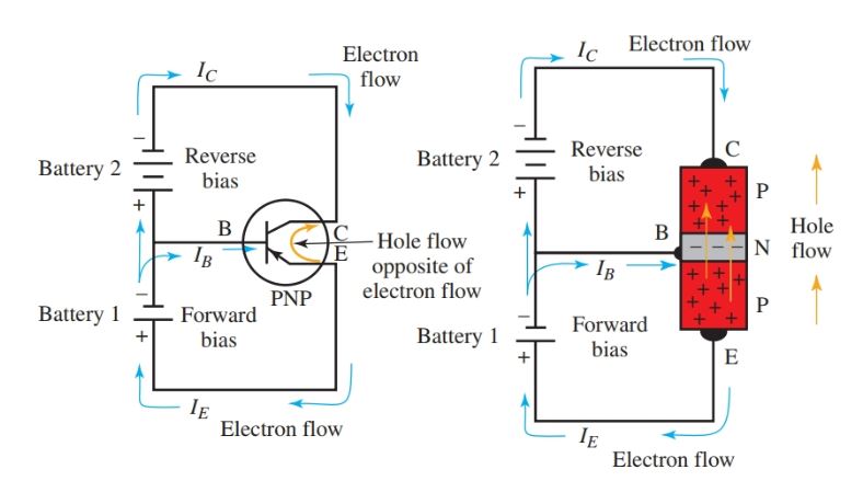
Figure 5. Forward and reverse bias in a PNP transistor amplifier circuit.
Single Battery Circuit
Two voltage sources have been used in all circuits discussed thus far. One source was used for the forward biasing of the emitter junction, and the other source was used for the reverse biasing of the collector junction. There is no need for two batteries. The amplifier in Figure 6 uses only one battery.

Figure 6. This circuit uses a single power source.
- There is no question about the reverse bias of the collector junction. The collector, C, is connected through RC to the most positive point of the circuit, the positive supply terminal.
- The most negative point in the circuit is the ground, and it is connected directly to the negative terminal of VCC.
- Resistors RF and RB form a resistance voltage divider connected directly across VCC.
- The voltage at the base, B, is less positive than the positive terminal of VCC by the amount of the voltage drop across RF. It is positive with respect to the emitter, E. E is at the ground, which is the most negative point in the circuit.
- By using the proper values for RF and RB, the desired forward bias voltage and current can be established in the emitter junction.
- The series resistance combination of RF and RB must be large enough so that the current drain from the supply battery is small. This ensures a long battery life.
Biasing Methods
The fixed bias method is shown in Figure 7. Notice that the resistor RB has been omitted. This circuit sets a constant base current. This bias is used for switching circuits.
A switch is inserted in the base to control current through the emitter-collector. Proper selection of R (RF and RC) sets up the required forward bias voltages and base current.
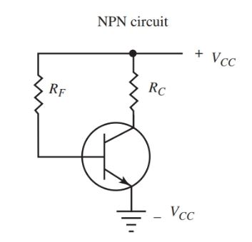
Figure 7. Fixed bias method for connecting a transistor.
The single battery bias scheme is another common method for biasing transistors, Figure 8.
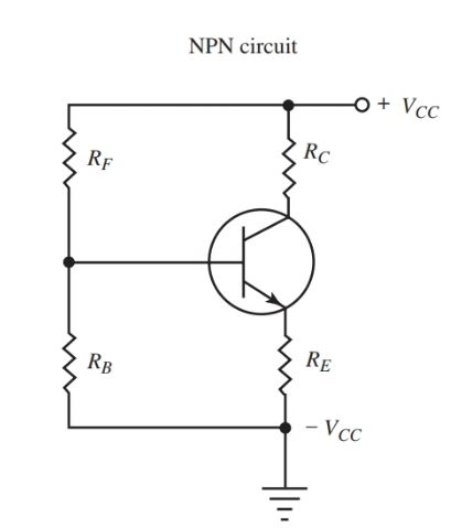
Figure 8. Schematic of single battery bias
Emitter biasing is a third method for setting forward bias of the emitter junction, Figure 9. In this case, the forward bias voltage VEE will set a constant emitter current, IE. This produces a voltage drop across RE. RE is chosen to provide the proper forward bias and RB is the return to complete the emitter circuit.
An ac signal applied to the amplifier base will produce a larger ac component in the collector current. This does not upset the emitter bias, because a low-reactance path around RF is provided by bypass capacitor C.
This circuit ensures a stable operating point for the transistor. A disadvantage of this circuit, however, is the need for two power supplies or batteries.
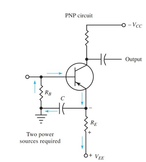
Figure 9. Schematic of the circuit for emitter biasing.
A self-bias schematic is shown in Figure 10. This circuit differs from the fixed bias method in that bias resistor RF is connected to the collector rather than to VCC. This method provides a more stable operating point than fixed biasing and requires only one power source.
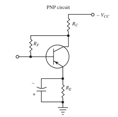
Figure 10. Schematic of the self-bias circuit.
If a fixed collector current is assumed at some operating point, the collector voltage, VC, will be constant. But it will be lower in value than VCC, due to the voltage drop across RC.
Any change in IC will also change the value of VC. Since the base is connected to VC through RE, a certain amount of degeneration will result.
What is meant by degeneration? A positive signal at the input of the PNP amplifier makes the base more positive, decreases it’s forward bias, and decreases IC.
A reduction in IC means a lesser voltage drop across RC. Collector voltage VC becomes more negative as it reaches the value of negative VCC. This more negative voltage through RF to the base tends to increase forward bias. It also opposes any increase caused by the input signal.
In a phase relationship that opposes the input, a signal from the output of a device fed back to the input is called degeneration. The major disadvantage of self-bias is the loss of amplifier gain due to degeneration.