The article provides an overview of semiconductor diode, covering their theory, types, and characteristics. It explains the structure and function of diodes, their forward and reverse biasing, different types such as rectifier, Zener, and light-emitting diodes (LEDs), and their practical applications, characteristics, and testing methods.
Diode Definition: A diode is a device designed to permit electron flow in one direction and block flow from the other direction. A diode consists of two electrodes: a cathode and an anode. A cathode is an electrode that emits (gives off) electrons. An anode collects the electrons and puts them to use.
Semiconductor Diode Definition: A semiconductor diode is the result of the fusion between a small N-type crystal and a P-type crystal, Figure 1. At the junction of the two crystals, the carriers (electrons and holes) tend to diffuse. Some electrons move across the barrier to join holes. Some holes move across the barrier to join electrons. Remember that unlike charges attract each other.
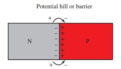
Figure 1. A semiconductor diode made of N-type and P-type crystals.
Due to this diffusion, a small voltage, or potential, exists between the regions near the junction. How does this happen?
The region of the P crystal near the junction becomes negative. It has taken electrons from the N crystal. The region of the N crystal near the junction becomes positive. It has lost some electrons but gained holes. This voltage or potential is called a potential hill or a potential barrier. The barrier prevents the other electrons and holes in the crystal from joining.
Semiconductor Diode Symbol
The symbol for a semiconductor diode is shown in Figure 2. The arrow side of the symbol denotes the anode portion of the diode. The anode contains the P-type material. The bar side of the symbol denotes the cathode portion of the diode. The cathode contains the N-type material.
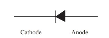
Figure 2. Symbol for a semiconductor diode.
Forward and Reverse Biasing
A voltage (potential) is connected across a diode in Figure 3. The positive terminal of the source is connected to the P crystal. The negative source is connected to the N crystal.
Forward Bias
The negative electrons in the N crystal move toward the barrier. The positive holes in the P crystal move toward the barrier. The source voltage opposes the potential barrier and reduces its barrier effect. This allows the electrons and holes to join at the barrier. Therefore, current flows in the circuit. It flows in the P crystal by holes. It flows in the N crystal by electrons. The diode is biased in a forward direction, or forward biased.
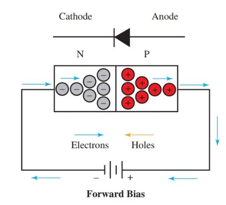
Figure 3. Conduction through a junction diode biased in the forward direction.
There is a minimum forward biased voltage needed to overcome the potential barrier for current to flow in the circuit. This minimum voltage depends on the type of semiconductor material used.
It requires approximately 0.6 volts of potential to forward bias a silicon diode and 0.2 volts for a germanium diode. Once this barrier voltage is exceeded, current flows through the circuit.
Reverse Bias
Figure 4 the positive source is connected to the N crystal and the negative source is connected to the P crystal. This shows the same junction diode biased in a reverse direction, or reverse biased.
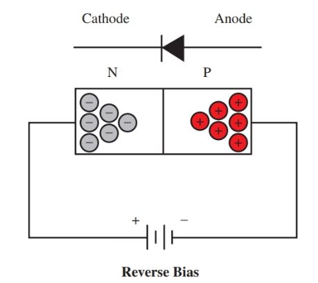
Figure 4. No conduction through a junction diode biased in a reverse direction.
In reverse bias, the source voltage aids the potential barrier. Electron/hole combinations are limited at the junction. The electrons in the N crystal are attracted to the positive source terminal. Very little current will flow in the circuit.
A reverse voltage can be increased to a point where the diode will break down. The amount of reverse bias will vary according to the diode specifications.
Types of Semiconductor Diode
Diodes are used for a number of purposes. Voltage rectification, voltage regulation, and even light production are some of their various uses. Following is a brief description of some diode types you might encounter.
Point Contact Diodes
The point contact diode is used for detection and rectification. It consists of a small piece of N-type germanium crystal. Against this crystal is pressed a fine phosphor bronze wire.
While the diode is being made, a high current is run through the diode from wire to the crystal. This forms a P-type region around the contact point in the germanium crystal. The point contact diode, therefore, has both the P- and N-type crystals. Its operation is like that of the junction diode.
Silicon Rectifiers
Diodes conduct current more easily in one direction than in the other. This process is used to produce rectification. A key semiconductor diode is the silicon rectifier.
Figure 5 shows two typical rectifiers. However, silicon rectifiers come in a wide variety of shapes and sizes. Figure 6 shows some common diode outlines.
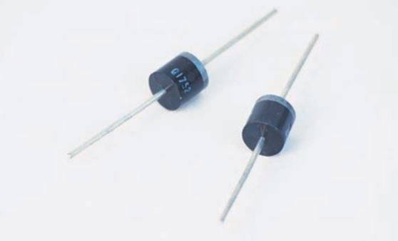
Figure 5. Typical rectifier diodes.
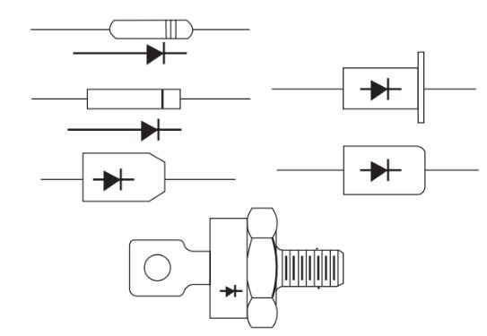
Figure 6. Some widely used silicon rectifier outlines.
Silicon rectifiers have high forward-to-reverse current ratios. This is the ratio of current allowed in the forward direction compared to the current allowed in the reverse direction.
They can achieve rectification efficiencies of greater than 99 percent. These rectifiers are very small, light, and built to last a long time.
In addition, they can be made resistant to shock and mishandling. Silicon rectifiers do not decay with age as a vacuum tube rectifier does.
Zener Diodes
An electronic device that can be used as a voltage regulator is the Zener diode, Figure 7.
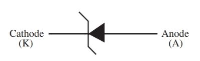
Figure 7. The schematic symbol for the Zener diode.
Characteristics Curve
Figure 8 shows a characteristic curve for a Zener diode. When the diode is forward biased, it acts like a diode or a closed switch.
However, the Zener has unique reverse bias qualities that make it differ from the typical diode. The Zener will go into reverse bias at various voltages.
The amount of voltage required for reverse bias varies according to the Zener diode selected. Some typical reverse bias voltages are 2.4 V, 5.1 V, 6.0 V, 9.1 V, 12.0 V, etc. At this point, when the applied voltage is increased, the forward current increases. This small reverse current flows until the diode reaches the Zener breakdown point, V2 in Figure 8.
At the Zener breakdown point, the Zener diode is able to maintain a fairly constant voltage as the current varies over a certain range. Because of this attribute, the diode provides excellent voltage regulation. Figure 9 shows a Zener diode is used as a simple shunt regulator.
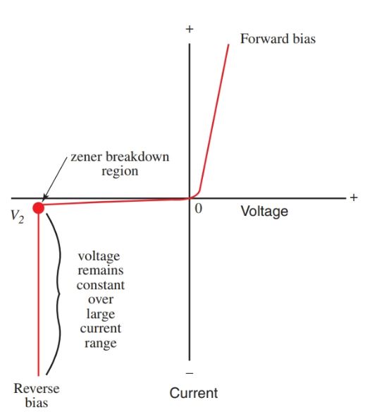
Figure 8. Zener diode characteristics curve
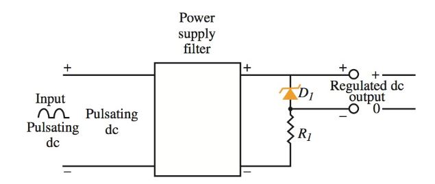
Figure 9. Zener diode as a shunt voltage regulator.
Light Emitting Diodes
The light emitting diodes (LED) is a special function diode, Figure 10. When connected in the forward bias direction, it emits light. Light emitting diodes are made from semiconductor compounds such as gallium arsenide, gallium arsenide phosphide, and gallium phosphide.
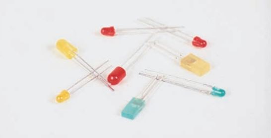
Figure 10. Various LEDs.
An LED receives energy from a dc power supply or a battery. This causes the electrons and holes to combine in the PN junction region of the diode. This combination creates photons, which are “particles” of light that can be seen.
Each photon is produced from one hole (+ charge) and one electron (– charge). Different LED colors are achieved by using different materials in the manufacture of the LED.
Figure 11 shows the operating principle of an LED. The LED must be connected to a power source with some form of resistance in series with the LED. If the LED is connected directly to a source with forward bias, the LED will be destroyed.
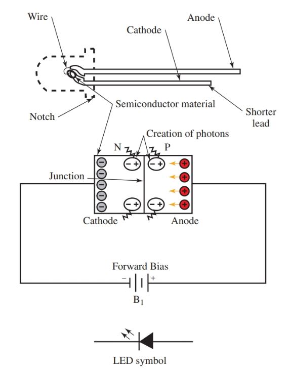
Figure 11. LED operation.
LED Biasing
Biasing diagrams for some common LEDs are shown in Figure 12. Note that the cathode lead is the shortest lead. It is also closest to the notch on certain diodes.
LEDs have many uses. For example, they are used on the instrument panel of cars, clocks, watches, and many other electric devices.
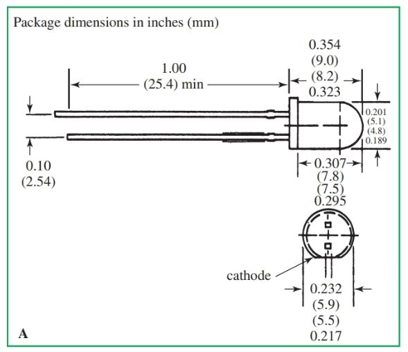
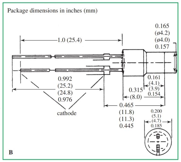
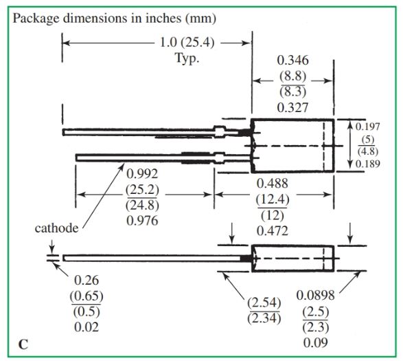
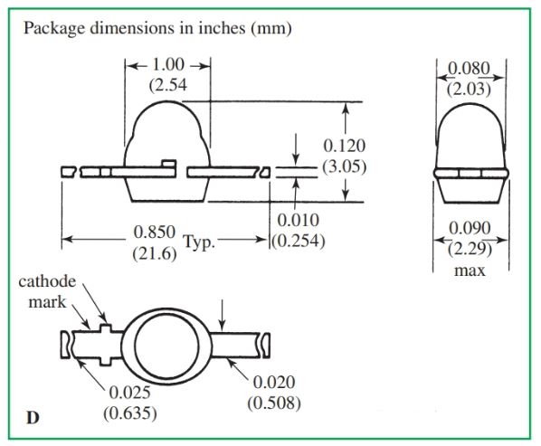
Figure 12. LED biasing diagrams. A–T 1 3/4 LED lamp. B–Cylindrical LED lamp. C–Rectangular LED lamp. D–Miniature axial lead LED lamp. (Siemens)
Diode Characteristics and Ratings
Ratings of diodes and rectifiers are commonly based on current and voltage capabilities and peak inverse voltage.
Peak Inverse Voltage
The peak inverse voltage (PIV) rating used by manufacturers defines the greatest reverse voltage that can be applied across a rectifier without damaging it. An example of this is one amp at 50 PIV for a 1N4001 silicon rectifier. This means that a 1N4001 silicon rectifier can withstand a maximum applied reverse voltage of 50 volts.
Many diodes are identified by a “1N.” Examples of this are 1N4001 or 1N5400. Some manufacturers use their own labels: HEP 320, SK 3051, or 276-1102.
Testing Diodes
You have learned that diodes with a forward bias direction have a low resistance to current flow. A reverse bias direction has a high resistance. This allows diodes to be tested using an ohmmeter.
To test a diode in the forward bias direction, connect the diode across the ohmmeter. Set the range switch on the low resistance setting (×1 or ×10). The reading should be low. A low reading is from 50 to 1000 ohms. See Figure 13, part A.
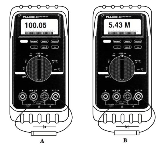
Figure 13. Testing a diode using an ohmmeter. A–Testing forward bias. B–Testing reverse bias.
To test a diode in the reverse bias direction, connect the diode across the ohmmeter leads. Set the range switch on a high resistance setting, such as ×10 k, ×100 k, or ×1 M. A good diode will show a very high resistance. See Figure 13, part B.
Many new digital meters have a diode test function built in. One model with a diode symbol on the selector switch is shown in Figure 14. A properly connected diode can be tested by turning the switch to the diode function.
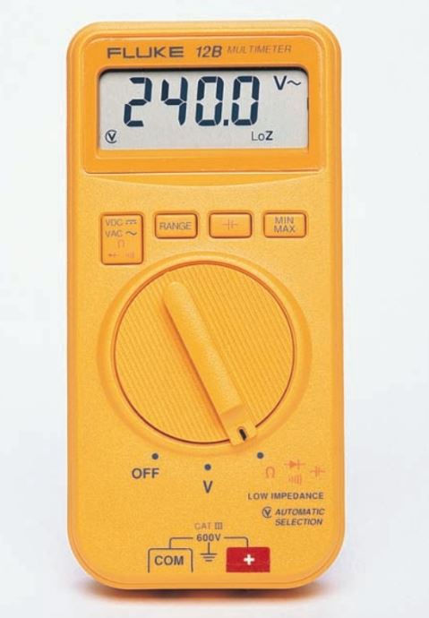
Figure 14. This digital meter can also be used to test diodes. (Fluke Corp.)