The article explains the operation of a digital to analog converter and examines the key performance characteristics that govern how digital data is translated into continuous analog signals.
An analog-to-digital converter (ADC) is a device for converting continuous-time analog signals to digital signals. A digital-to-analog (D/A) converter is a device that converts digital signals, represented as discrete binary values, into continuous analog signals.
The discrete values could represent audio samples, sensor readings, control values, or any other form of digitally encoded information. The D/A converter takes the digital input and converts it into an analog signal that varies continuously based on the digital value. Most microcontrollers do not have a D/A converter, but the function of the D/A converter is approximated on microcontrollers using the PWM output feature.
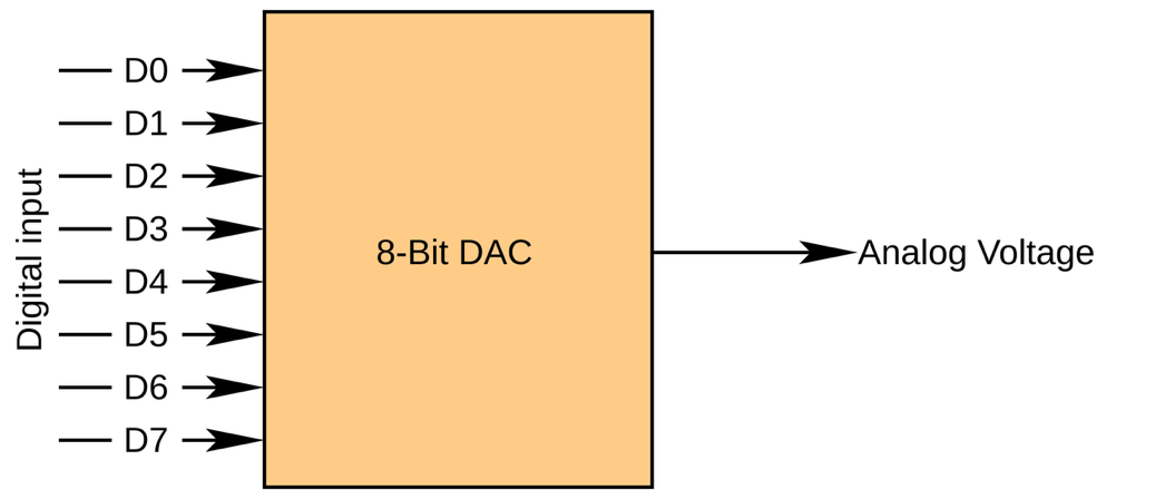
Figure 1. Functional Diagram of an 8-bit Digital to Analog Converter
Digital to Analog Converter Characteristics
The performance of a digital-to-analog converter is defined by several key characteristics that determine how accurately and how quickly digital data can be reconstructed into a continuous-time analog signal. The most important DAC characteristics include conversion rate, output voltage range, bit resolution, and quantization error.
Conversion Rate
The conversion rate of a DAC, often referred to as the update rate or settling rate, indicates how frequently the digital input code can be converted into a new analog output value. It is typically specified in samples per second (S/s).
In control and signal-generation applications, the conversion rate determines how smoothly the output waveform can be reconstructed and how fast the DAC can respond to changes in the digital input. In practice, the effective update rate may be limited by interface speed, output settling time, and the bandwidth of the analog output stage.
Voltage Range
The output voltage range defines the minimum and maximum analog voltage that the DAC can produce. This range is usually determined by an internal or external reference voltage.
For example, a DAC with a 0 to 5 V output range maps the full digital code range to this voltage span. Some DACs support bipolar output ranges (such as ±5 V or ±10 V) through additional output circuitry. The selected output range directly affects the voltage resolution of the DAC and must be matched to the requirements of the driven load or control system.
Bit Resolution
The bit resolution of a DAC specifies the number of discrete output levels available to represent the analog signal. A DAC with n bits can produce 2n distinct output levels.
Higher resolution allows finer control of the output voltage and reduces the size of each voltage step. Common DAC resolutions range from 8 to 16 bits in embedded systems, while precision instrumentation DACs may offer 18 bits or more. The voltage resolution of a DAC is given by:
$$\text{Voltage Resolution} = \frac{\text{Output Range}}{2^n}$$
This resolution represents the smallest change in output voltage that can be produced by changing the digital input code by one least significant bit (LSB).
Quantization Error
Quantization error in a DAC arises because a continuous analog range is represented by a finite number of discrete output levels. As a result, the actual analog output can deviate from the ideal value corresponding to the digital input code.
The inherent quantization error of a DAC is typically ±½ LSB. This error sets a fundamental limit on output accuracy, even before considering other non-ideal effects such as offset error, gain error, and nonlinearity. In precision applications, these additional errors must be considered alongside quantization effects to assess overall DAC performance.
Example 1 discusses the mapping between digital input values and analog output values.
Example 1 D/A Mapping
A 3-bit D/A converter is set for a 0 to 10 V output range. Map all the possible digital input values to their corresponding analog output values.
Solution
A 3-bit D/A converter has 23 possible digital input values (0 to 7 decimal or 000 to 111 binary). The voltage resolution is 10/23 = 1.25V . The corresponding analog output values for each possible digital input value are shown here:
| Binary Input | Analog Output (V) |
| 000 | 0.00 |
| 001 | 1.25 |
| 010 | 2.50 |
| 011 | 3.75 |
| 100 | 5.00 |
| 101 | 6.25 |
| 110 | 7.50 |
| 111 | 8.75 |
Note that while this D/A converter’s nominal range is 0 to 10 V, the maximum output analog value is only 8.75 V due to the coarseness of its resolution. If the bit resolution was 10 instead of 3, then the maximum analog output voltage would be 9.990 V, or to generalize
$$ \textrm{Maximum Output}=range – resolution = 10-\frac{10}{2^{10}}=9.990V$$
For a D/A converter, the digital input that gives a certain analog output voltage Vout is given by
$$ \textrm{Digital Input}=ceiling(\frac{V_{out}-V_{in}-\textrm{Voltage Resolution}}{\textrm{Voltage Resolution}}) (1)$$
where Vmin is the minimum voltage supplied by the D/A. For example, using the data from Example 1, the digital input needs to be 6 for an output of 8 V. Due to the coarse resolution of this A/D converter, the analog output will only be 7.5 V (6 × 1.25). If this were a 10-bit D/A converter instead, then the output would be 7.998 V at a digital input of 819. Most commercial D/A converters have a 12-bit output resolution.
Digital to Analog Converter Operation
To illustrate the operation of a D/A converter, let us consider the weighted resistor summing amplifier circuit shown in Figure 2. The digital input acts as an electronic switch in this circuit, providing a connection between VR and the respective resistor if the binary value is 1. For the digital input 1011 shown in the figure, the output of this circuit is -11VR. This circuit is not used in practice, because it requires resistances of certain ratios which are difficult to satisfy with good accuracy. This is especially true for a D/A converter with more than 4 bits. For example, a 12-bit D/A would require that the 11th-bit resistor have a resistance of 1/2048 of the 0th-bit resistor.
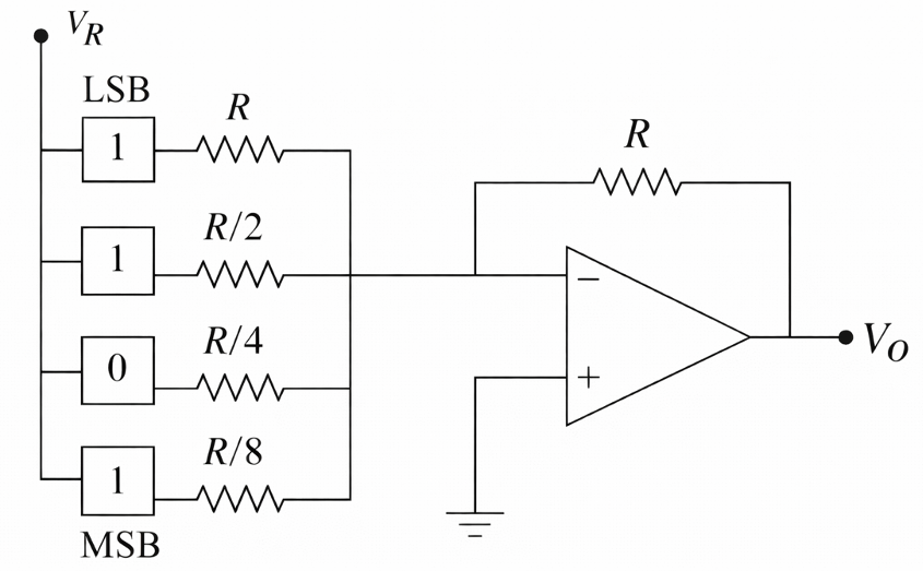
Figure 2. Weighted resistor summing amplifier circuit
A commonly used circuit for D/A conversion is the R/2R ladder resistor network. Unlike the weighted resistor summing amplifier circuit, the R/2R ladder circuit requires only two resistor values R and 2R regardless of the number of bits. The R/2R ladder circuit is shown in Figure 3. It consists of a repeating pattern of 2R and R resistors arranged in a ladder form. The 2R termination resistor is connected to the ground and is used to make the Thevenin resistance of the network at each ladder leg equal to R when all the bits are grounded (see Figure 3).
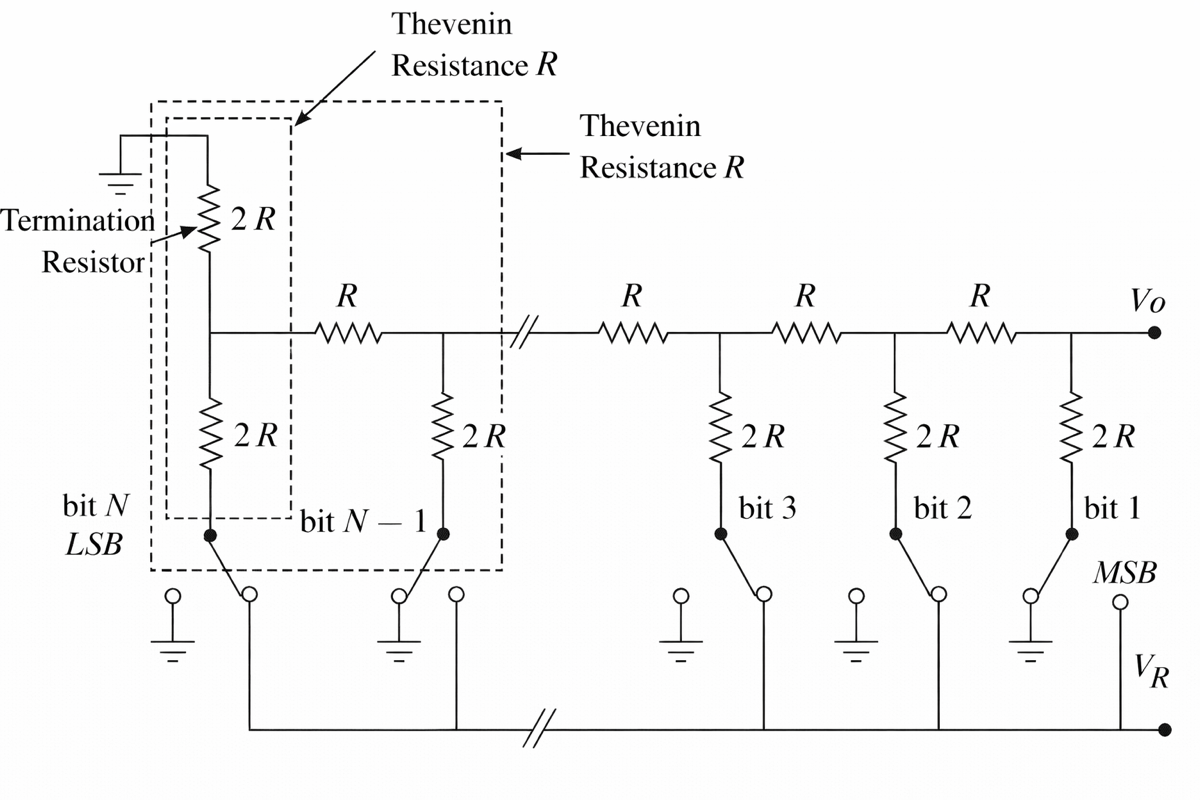
Figure 3. R/2R ladder resistor network
The output voltage Vo when a voltage VR is connected to a bit $ i(1\leq i\leq N) $ with all the other bits grounded is given as
$$ V_{o}=\frac{V_{R}}{2^{i}} (2)$$
If more than one bit is connected to VR , then the principle of superposition applies. Thus, for example, if we have a 3-bit D/A with all the bits connected to VR, then the analog output is equal to $ V_{R}/2+V_{R}/4+V_{R}/8=7/8V_{R} $. If VR is equal to 10 V, then the output is 8.75 V, as was the case in Example 1. The R/2R network provides the most accurate method of digital-to-analog conversion.
Practical D/A converters employ a Zero-Order Hold (ZOH). After a digital value is converted to an analog value by the D/A converter, the ZOH ensures this analog value remains constant until the next digital value is received and converted. This means that the current output of the D/A device will remain constant until a new output is sent to the device.
Key Takeaways
Understanding digital-to-analog converter operation and characteristics is essential because DACs form the bridge between digital computation and the analog world in which most physical systems operate. Conversion rate, voltage range, resolution, and quantization error directly influence signal fidelity, control accuracy, and system stability in applications ranging from motor drives and power electronics to instrumentation, audio systems, and industrial control. Knowledge of practical DAC implementations, such as R/2R ladders and zero-order hold behavior, allows engineers to anticipate real-world limitations and select appropriate devices or architectures.