This article explains the operation and key characteristics of an analog to digital converter (ADC), including sampling, quantization, resolution, conversion methods, and performance limits. It also describes common ADC architectures and input signal configurations, highlighting how these choices affect accuracy, noise immunity, and practical data acquisition in embedded and measurement systems.
An analog-to-digital (A/D) converter is a hardware device for converting continuous-time analog signals to digital signals. An A/D converter operates as follows.
- The continuous-time analog signal is first sampled at regular intervals, which involves measuring the instantaneous value of the signal at discrete points in time.
- Once a sample is acquired, the sample-and-hold circuit of the A/D converter becomes active. This circuit maintains the sampled value constant throughout the sampling interval. Its primary role is to provide a steady value to the quantizer, ensuring that variations in the analog signal during the quantization process do not introduce errors.
- The held value is then quantized to represent it digitally. Quantization involves approximating the continuous range of the analog signal into a finite set of discrete levels.
The outcome of the A/D conversion process is a series of discrete digital values, which effectively represent the original continuous-time analog signal in a discrete format.
Analog to Digital Converter (ADC) Characteristics
Among the critical characteristics of an A/D converter are its conversion rate, voltage range, bit resolution, and quantization error.
The conversion rate indicates how many analog-to-digital conversions are performed within a specified time unit, typically a second. On a microcontroller, this rate hinges on the selected clock signal, its speed, and the chosen bit range. A/D devices embedded in PC data acquisition cards typically exhibit conversion rates of under 100,000 conversions per second for entry-level models. In contrast, advanced models can achieve rates exceeding one million conversions per second. It is essential to understand that these figures represent the peak performance capabilities of the standalone A/D device. When integrating an A/D converter into a digital feedback control system, the effective conversion rate tends to decrease, primarily influenced by the processing speed of the system.
The voltage range of an A/D converter refers to the analog voltage range that the device can handle. On a microcontroller, the range is 0 to VDD (the supply voltage) unless an external reference voltage (AREF) is used, in which case the range is 0 to AREF. On a PC data acquisition card, most A/D devices allow both unipolar and bipolar ranges, ranging from 0.05 to 10 V, but can tolerate an overload voltage of up to 30 V. The voltage conversion range is normally set by a software call to the device controller.
The bit resolution of the A/D device is quoted as the number of bits that the converted analog signal is mapped into. Common bit sizes are 12 to 16 bits, but many microcontrollers have A/D devices that have only a 10-bit range. The bit resolution affects the voltage resolution or increment of the device, which is shown in the formula
$$\textrm{Voltage Regulation}=\frac{Range}{2^{n}}$$
where n is the bit resolution of the A/D converter. To understand the relationship between voltage range and voltage resolution, let us consider a 12-bit A/D device with a –10 to 10 V range. In this case, a 20-V range (–10 to 10 V) is mapped into 212 binary combinations. Thus, the device can map voltage values to discrete values at increments of
$$ \frac{Range}{2^{n}}=\frac{20}{4096}=4.88 \textrm{ mV} (1) $$
This means that the input voltage can increase by up to 4.88 mV without changing the output value of the A/D converter. For example, if the input voltage that was measured by this device was the output of an analog temperature sensor with a sensitivity of 10 degrees per volt (o/V), then the device will not be able to measure temperature changes that are less than 0.0488o. The discrete output of an A/D converter subjected to an input voltage Vin is given by
$$\textrm{Digital Output}=ceiling(V_{in}-V_{ref}-\textrm{voltage resolution})/\textrm{voltage resolution} (2) $$
Where Vref is the reference voltage for the A/D, which is typically zero volts.
Along with the voltage resolution of the device, the quantization error (or digitization accuracy) of the A/D converter is also an important performance parameter and is directly related to the bit range of the device. The digitization accuracy refers to the uncertainty in the discretized voltage value, and it is +/− one-half of a bit. To further understand the concept of digitization accuracy, let us consider a contrived 2-bit A/D device with a range of 0 to 5 V. This A/D device maps a 5 V analog range (0 to 5 V) into four different binary values ( 2n or 0, 1, 2, and 3). As seen in Figure 1, the output of the A/D converter will be 0 if the input analog voltage happens to be in the range of 0 to 1.25 V, 1 if the input analog voltage happens to be in the range of 1.25 to 2.5 V, and so forth. Notice that the maximum digital output level (3 in this case) is reached before the input reaches full scale or 5 V. Nominally, we say that if the A/D converter outputs a value of 1, then this corresponds to a nominal analog voltage of 1.875 V.
The input voltage can change up to +/−0.625 V (or +/− one-half of a bit) without any change in the output of the A/D. Thus, at any of the discrete output values of the A/D converter, we say that we have an uncertainty of +/− half the voltage increment of the A/D device. Some A/D converters are built with an intentional offset of −1/2 bit. The staircase output curve of such a device will be shifted to the left and will start at 0.625 V for the 2-bit A/D example. The input/output relationship of an A/D converter is further illustrated in Example 1.
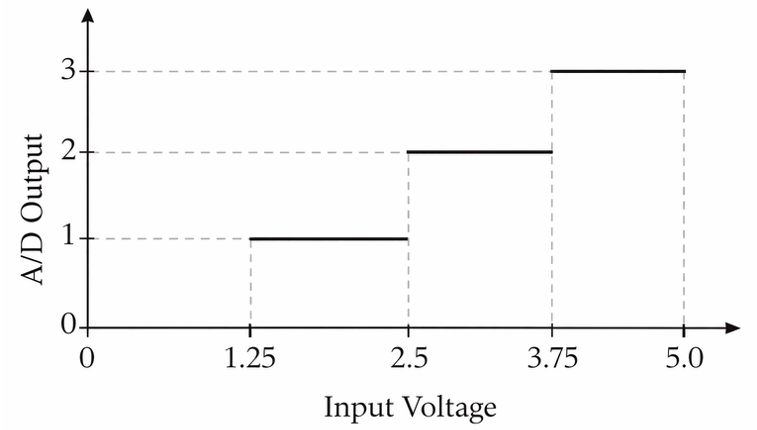
Figure 1. Two-bit A/D Mapping
Example 1 A/D Converter
Determine the voltage resolution and digitization accuracy of a 12-bit A/D converter with a 0 to 10 V range. Determine the output level if the input voltage is 6.5 V. Also, determine the corresponding analog input voltage at the following digital output values: 0 and 1000.
Solution
From Equation (1), the voltage resolution of this A/D device is 10/212 = 2.441 mV. Thus, the digitization accuracy of the conversion is +/− 1.220 mV.
From Equation (2), the discrete output level is given as the integer ceiling of ((6.5 V – 2.441 mV)/2.441 mV) or 2662.
This 12-bit A/D converter maps the 0 to 10 analog voltage range into 0 to 4095 digital values. When the A/D converter outputs a value of 0, the analog input voltage of this A/D converter is in the range of 0 × 2.441 mV to 1 × 2.441 mV or 0 to 2.441 mV. Similarly, when the A/D converter outputs a value of 1000, the analog input voltage is in the range of 1000 × 2.441 mV to 1001 × 2.441 mV or 2.441 to 2.443 V.
Analog to Digital Converter (ADC) Operation
Most A/D converters are built to operate on the principle of successive approximation. In the Successive approximation method, an internal digital-to-analog (D/A) converter and a comparator circuit are used to converge on the digital signal that is closest to the sampled analog signal. Starting with the MSB, the bits in the D/A converter are set/reset one at a time until the sampled analog signal matches the output signal from the D/A converter to within the least significant bit. The binary pattern of the D/A converter is then the digital input signal. This conversion technique is a good compromise between speed, resolution, and cost.
Example 2 illustrates the operation of a successive approximation 3-bit A/D converter with a 0 to 10 V analog input range. Other types of A/D converters include flash/parallel, integrating, and digital ramp.
Most microcontrollers have several A/D channels. On a PC, the A/D converter is packaged with a digital-to-analog converter and a parallel port to form a data acquisition card. The card is placed in one of the available computer slots, and a cable then is used to connect the card to an interface board commonly known as a distribution panel or screw terminal. To set up an A/D converter in a PC data acquisition board, the user has to make certain important selections, including the input range and the input signal configuration. The input range is normally set using software.
Example 2 Successive Approximation A/D
Illustrate the operation of a 3-bit, 0 to 10 V successive approximation A/D subjected to an analog input voltage of 8 V.
Solution
With reference to Figure 2, the control logic of this A/D device will first turn the most significant bit (bit D2) of the internal D/A device associated with this A/D. The analog output voltage corresponding to this bit is 5 V (see Table 1).
The comparator circuit will then compare the analog output of the internal D/A with the supplied analog input (8 V). Since the output of the internal D/A is smaller than the supplied voltage, bit D2 remains on, and the next bit (bit D1) is turned ON. The analog output (7.5 V) of the internal D/A is still less than the supplied voltage, so bit D1 remains ON. When bit D0 is turned ON, the analog output is 8.75 V, which is greater than the supplied voltage. Thus, bit D0 is turned OFF, and the output of the A/D will be 0x06, which is the same digital pattern on the internal D/A.
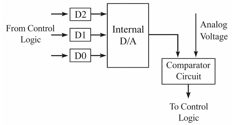
Figure 2. Three-bit successive approximation A/D
| Binary Input | Analog Output (V) |
| 000 | 0.00 |
| 001 | 1.25 |
| 010 | 2.50 |
| 011 | 3.75 |
| 100 | 5.00 |
| 101 | 6.25 |
| 110 | 7.50 |
| 111 | 8.75 |
Table 1. Analog Outputs and Corresponding Binary Inputs
Analog to Digital Converter Input Signal Configuration
The configuration of an A/D input signal is classified into two types: single-ended input and differential input.
Single-Ended Input Mode
In the single-ended input mode, the input signal is referenced to the A/D board’s signal ground. As illustrated in Figure 3(a), the signal is transmitted using two wires. The wire carrying the signal is connected to any of the input channel terminals, while the other wire is linked to the board’s signal ground, often referred to as low-level ground or LLGND. In this setup, the A/D converter determines the difference between the signal and the board’s ground. However, a single-ended connection is prone to noise since the signal wire can inadvertently function as an antenna, capturing electrical interference.
It is essential to note that the single-ended configuration is suitable only for floating signal sources to prevent ground loops (as explained in Section 2.10). A floating signal source is not connected to any common ground or fixed potential, and lacks any ground connection at the signal source. Battery-powered devices are typical examples of floating signal sources. Being independent of an external power source or ground, their signal outputs remain unanchored to a reference point.
Differential Input Mode
In the differential input mode, the high (or positive) input signal’s value is ascertained relative to the low input (or negative) signal. Typically, three wires are used for connection to the board. The wire conveying the high-input signal is connected to one of the A/D input channel terminals, for instance, 0, 1, 2, …, 7 (assuming 16 single-input channels exist). The low signal connects to an adjacent channel, like channel 8 in Figure 3(b) if the main signal connects to channel 0. This low signal wire also joins the board’s signal ground via a resistor. When set to the differential input mode, the total number of usable input channels is reduced by half. Thus, a board with 16 single-ended input channels will offer only eight channels in differential mode.
Differential input mode boasts superior noise handling compared to its single-ended counterpart. Electromagnetic interference typically affects both leads of the signal. Since the A/D converter in differential mode gauges the discrepancy between the high and low inputs, voltages common to both inputs are effectively negated. This mode is particularly recommended for reading outputs from analog sensors prone to noise, such as thermocouples and strain gauges. A measure of the ability of an A/D converter used in differential input mode to eliminate the common voltage is called the common mode rejection ratio (CMRR).
In an ideal A/D converter, any voltage common to both signal wires will be completely canceled. In a real A/D converter, a perfect cancellation does not occur, and a fraction of the common voltage will show. The CMRR, which is expressed in decibels (dB), is the reciprocal of the voltage fraction that is passed. It is desirable to have an A/D converter with a high CMRR ratio. Note that most MCUs do not support differential mode A/D input, but Microchip manufactures special A/D ICs that support differential A/D input. An example is the MCP3301 IC, which is a dedicated 13-bit differential input A/D converter IC.
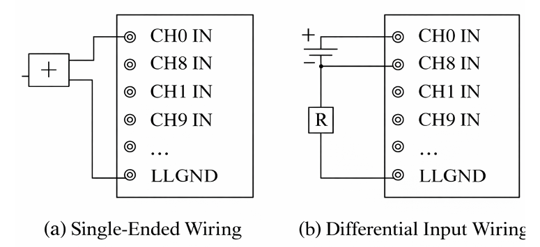
Figure 3. Data acquisition board wiring for single-ended and differential input mode
Key Takeaways
Understanding ADC operation, characteristics, and input configurations is essential for accurately interfacing real-world analog signals with digital systems. Proper selection of resolution, voltage range, conversion method, and input mode directly affects measurement accuracy, noise immunity, and system responsiveness in applications such as sensors, control systems, data acquisition, and embedded electronics. By applying these concepts correctly, engineers can ensure reliable signal capture and effective digital processing across a wide range of industrial, scientific, and consumer applications.