This article explores the operating regions of a bipolar junction transistor (BJT), including the active, cutoff, and saturation regions. It also discusses the process of developing characteristic curves to better understand transistor behavior.
Operating Regions of BJT
A collector family of characteristic curves is used to show the desirable operating regions of a transistor. The center area is called the active region. This area is located anywhere between the two shaded areas of Figure 1. Amplification is achieved when the transistor operates in this region.
A second possible region of operation is called the cutoff region. On the family of curves, this is where $I_{C} = 0$ mA. When a transistor is cut off, no $I_{B}$ or $I_{C}$ flows. Any current flow that occurs in this region is due to leakage current. As a general rule, a transistor operating in the cutoff region responds as a circuit with an open switch. When a transistor is cut off, there is infinite resistance between the emitter and collector.
The shaded area on the left side of the family of curves is called the saturation region. This area of operation is where the maximum $I_{C}$ flows. A transistor operating in this region responds as a closed switch. A transistor is considered to be fully conductive in the saturation region. The resistance between emitter and collector is extremely small when a transistor is saturated.
The response of a transistor in the three regions of operation is shown in Figure 2. In Figure 2(a), the transistor is operating in the active region. The value of $V_{CE}$ is somewhat less than that of the source voltage $V_{CC}$. Collector current through the transistor causes a voltage drop across $R_{C}$. The base current of a transistor operating in this region would be some moderate value between zero and saturation. Transistor amplifiers usually operate in this area.
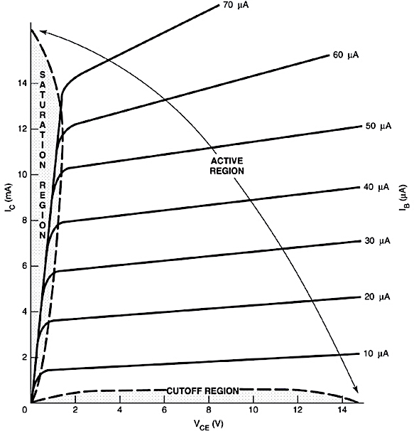
Figure 1. Operating regions of a transistor.
The response of a transistor when it is in the cutoff region is shown in Figure 2(b). In this condition of operation, the transistor responds as an open switch. With no current flow through the transistor, there is no voltage drop across $R_{C}$. $V_{CE}$ of this circuit is, therefore, the same as the source voltage ($V_{CE} = V_{CC}$). A transistor is cut off when no $I_{C}$ flows.
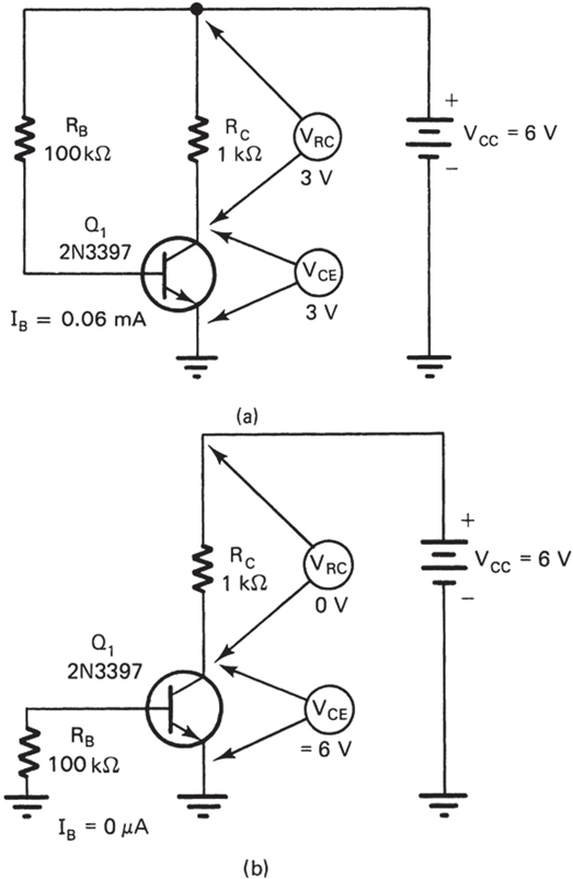
Figure 2. Transistor operation by Region: (a) Active Region, (b) Cutoff Region, (c) Saturation Region
Figure 2(c) shows how a transistor operates in the saturation region. In this condition of operation, the transistor responds as a closed switch. $V_{CE}$ is approximately equal to $0$ V. Heavy $I_{C}$ values cause nearly all of $V_{CC}$ to appear across $R_{C}$. In a sense, $V_{CE}$ is considered to be at ground. Current passing through the transistor is limited by the value of $V_{CC}$ and $R_{C}$. A large value of $I_{B}$ is needed to cause a transistor to saturate.
BJT Operating Regions Comparison
| Parameter | Active Region | Cut-off Region | Saturation Region |
| Base-Emitter Junction | Forward biased (≈ 0.6–0.7 V for Si) | Reverse biased | Forward biased |
| Base-Collector Junction | Reverse biased | Reverse biased | Forward biased |
| Collector Current (IC) | ≈ β × IB (controlled by base current) | ≈ 0 A (transistor OFF) | High (limited by circuit), not proportional to IB |
| Collector-Emitter Voltage (VCE) | Moderate (> VCE(sat), typically 0.7 V–VCC) | ≈ VCC (open circuit) | Very low (VCE(sat) ≈ 0.1–0.3 V for Si) |
| Input (Base) Current | Small but significant (controls IC) | ≈ 0 | Higher than in the active region |
| Power Dissipation | Moderate (P ≈ VCE × IC) | Minimal | High (due to high IC and low VCE) |
| Signal Behavior | Acts as an amplifier (linear region) | Transistor OFF (open switch) | Transistor ON (closed switch) |
| Typical Application | Analog amplifiers (voltage/current gain) | Digital logic “0” / switch OFF | Digital logic “1” / switch ON |
Developing Characteristic Curves of BJTs
Special circuits are used to obtain the data for a collector family of characteristic curves. Figure 3 shows a test circuit that is used to find the data points of a collector family of characteristic curves. Three meters are used to monitor this information. Base current and collector current are observed by meters connected in series with the base and collector. Collector-emitter voltage is measured with a voltmeter connected across these two terminals. $V_{CE}$ is adjusted to different values by a variable power supply.
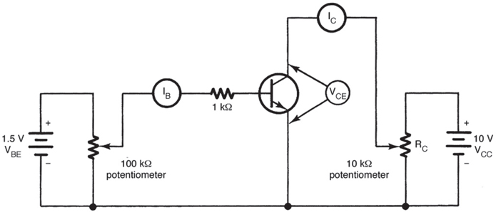
Figure 3. Transistor characteristic curve circuit.
The data points for a single curve are developed by first adjusting $I_{B}$ to a constant value. A representative value for a small-signal transistor is $10 , \mu A$. Resistor $R_{B}$ is used to adjust the value of $I_{B}$. The $V_{CE}$ is then adjusted through its range, starting at $0$ V. As $V_{CE}$ is increased in $0.1$-V steps to $1$ V, the $I_{C}$ increases very quickly. Corresponding $I_{C}$ and $V_{CE}$ values are plotted on the graph. $V_{CE}$ is then increased in $1$-V steps while $I_{C}$ is monitored. The resulting collector current usually levels off to a fairly constant value. The corresponding $I_{C}$ and $V_{CE}$ values are then added to the first data points. All points are then connected by a continuous line. The completed curve would be labeled $10 \mu A$ of $I_{B}$.
To develop the second curve, $V_{CE}$ is first returned to zero. $I_{B}$ is then increased to a new value. A common value for a small-signal transistor would be $20 \mu A$. The second curve is then plotted by recording the $I_{C}$ values for each $V_{CE}$ value.
To obtain a complete family of curves, the process is repeated for several other $I_{B}$ values. A representative family of curves may have 8-10 different $I_{B}$ values. The step values of $V_{CE}$ and the increments of $I_{B}$ and $I_{C}$ will change with different transistors. Small-signal transistors may use $10 , \mu A$ $I_{B}$ steps with $I_{C}$ values ranging from $0$ to $20$ mA. Large-signal transistors may use $1$-mA $I_{B}$ steps with $I_{C}$ values going to $100$ mA or more. Each transistor may require different values of $I_{B}$, $I_{C}$, and $V_{CE}$ to obtain a suitable curve.
Review Questions
- A collector family of characteristic curves for a bipolar transistor has 8 to 10 individual lines that represent different values of __________ current.
- The center area of a collector family of characteristic curves is called the __________ region.
- The area of a collector family of characteristic curves that shows where maximum $I_{C}$ flows represents the __________ region.
- The area of a collector family of characteristic curves that shows where no $I_{C}$ occurs is called the __________ region.
- When a transistor operates in the active region with a moderate value of $I_{B}$, the $V_{CE}$ will be (greater, less) __________ than the source voltage $V_{CC}$.
- When a transistor operates in the cutoff region, the $V_{CE}$ will be equal to the __________ voltage.
- When a transistor operates in the saturation region, the $V_{CE}$ will be approximately __________.
Answers
- Base
- Active
- Saturation
- Cutoff
- Less
- $V_{CC}$
- 0 V
Key Takeaways
BJTs have three operating regions—active, cutoff, and saturation. The active region is key for amplification, while the cutoff and saturation regions play roles in switching applications. Developing the characteristic curves of a transistor allows engineers to visualize the relationship between $V_{CE}$, $I_{C}$, and $I_{B}$, which helps in determining optimal operating conditions for various applications. This knowledge is fundamental to ensuring efficient transistor performance in both small-signal amplification and digital switching circuits.