This article describes the biasing techniques used for NPN and PNP transistors, including the conditions required for forward and reverse biasing and how these affect current flow and device performance.
NPN Transistor Biasing
The biasing of an NPN transistor is essential for its correct operation in electronic circuits. Consider the biasing of the NPN transistor shown in Figure 1. In this diagram, an external voltage source has been applied only to the emitter-base regions of the transistor. In an actual circuit, this source is called the emitter-base voltage, or $V_{BE}$.
Note that the polarity of $V_{BE}$ causes the emitter-base junction to be forward-biased. This condition forces majority current carriers together at the emitter-base junction. The resulting current flow in this case would be quite large. In this example, note that the same amount of current flows into the emitter and out of the base. Emitter current ($I_{E}$) and base current ($I_{B}$) are used to denote these values. Under normal circuit conditions, a $V_{BE}$ source would not be used independently.
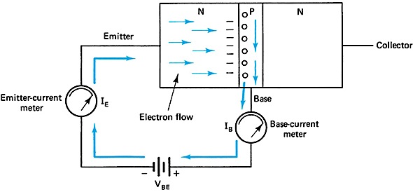
Figure 1. Emitter−base biasing.
Figure 2 shows an external voltage source connected across the base-collector junction of an NPN transistor. The base-collector voltage, or $V_{CB}$, is used to reverse-bias the base-collector junction. In this case, there is no indication of base current or collector current ($I_{C}$). In an actual reverse-biased junction, there could be a very minute amount of current, which is supported primarily by minority current carriers. As a general rule, this is called leakage current. In a silicon transistor, leakage current is usually considered to be negligible. In an actual circuit, $V_{CB}$ is not normally applied to a transistor without the $V_{BE}$ voltage source.
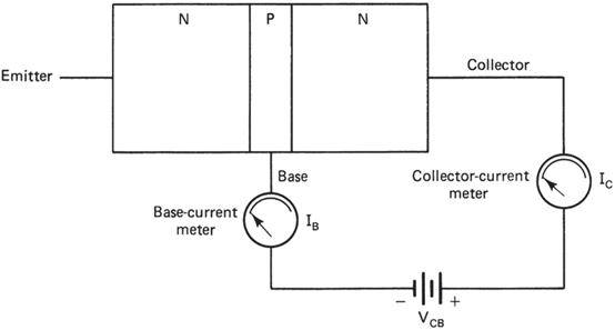
Figure 2. Base−collector biasing.
For a transistor to function properly, the emitter-base junction must be forward-biased, and the base-collector junction reverse-biased. Both junctions must have bias voltage applied at the same time. In some circuits, this voltage may be achieved by separate $V_{BE}$ and $V_{CB}$ sources. Other circuits may use a single battery with specially connected bias resistors. In either case, the transistor responds differently when all its terminals are biased.
Consider the action of a properly biased NPN transistor. Figure 3 shows separate $V_{BE}$ and $V_{CB}$ sources connected to the transistor. The $V_{BE}$ source provides forward bias for the emitter-base junction, whereas the $V_{CB}$ source reverse biases the collector junction. Connected in this manner, the two junctions do not respond as independent diodes.
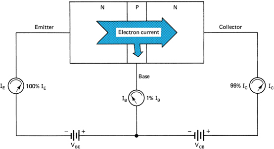
Figure 3. NPN transistor biasing circuit.
Figure 4 shows how current carriers pass through a properly biased NPN transistor. The forward-biased emitter-base junction causes a large amount of $I_{E}$ to move into the emitter-base junction. On arriving at the junction, a large number of the electrons do not effectively combine with holes in the base. The base is usually made very thin (0.0025 cm or 0.001”), and it is lightly doped. This means that the majority current carriers of the emitter exceed the majority carriers of the base. Most of the electrons that cross the junction do not combine with holes. They are, however, immediately influenced by the positive $V_{CB}$ voltage applied to the collector. A very high percentage of the original emitter current enters the collector. Typically, 95$\%$ to 99$\%$ of emitter current flows into the collector junction and becomes collector current.
After passing through the collector region, the collector current ($I_{C}$) combines with the base current ($I_{B}$) to ultimately form the emitter current ($I_{E}$). A large arrow indicates the current flow inside the transistor. Outside the transistor, small arrows indicate the base current.
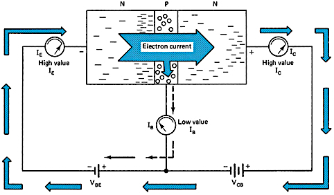
Figure 4. Current carriers passing through an NPN transistor.
The difference between the amount of emitter current and collector current of Figure 4 is equal to the amount of base current. Essentially, base current is due to the combining of a small number of electrons and holes in the emitter-base junction. In a typical circuit, base current is approximately 1$\%$ to 5$\%$ of emitter current. With the base region being very narrow, it cannot support a large number of current carriers. A small amount of base current is needed, however, to make the transistor operational. Note the direction of base current ($I_{B}$) and its flow path in the diagram.
The relationship of emitter current, base current, and collector current in a transistor is expressed by the following equation:
$$I_{E} = I_{B} + I_{C}$$
The largest current flow in a transistor takes place in the emitter. Collector current is slightly less than emitter current. This means that the current flow through a reverse-biased, collector-base junction is nearly equal to that of the forward-biased emitter-base junction. The difference in $I_{E}$ and $I_{C}$ is $I_{B}$.
If the base of a transistor were not made extremely thin and lightly doped, it would not respond as just described. The thin base region makes it possible for large amounts of emitter current to pass through the base and into the collector region. A thicker base would cause more emitter current to combine with holes in the base. Low doping of the base means that the majority current carriers of the emitter cannot effectively combine in the base. Instead of combining in the base, they pass through it and enter the collector. This improves the effectiveness of the base as a control element.
The amount of base current that flows in a transistor is very small but extremely important. Suppose, for example, that the base lead of the transistor in Figure 4 is momentarily disconnected. With this element open, it should be obvious that there will be no base current. Closer examination also shows that $V_{BE}$ and $V_{CB}$ are now connected in series. This means that their voltages are added together. As a result, the collector becomes more positive and the emitter more negative. One would immediately think that this condition would cause the transistor to conduct very heavily. However, it does not permit any conduction at all. In effect, this means that base current has a direct influence on emitter and collector current. The base-emitter junction of a transistor must be forward-biased for it to produce collector current.
PNP Transistor Biasing
Biasing of a PNP transistor is very similar to that of the NPN transistor. The emitter−base junction must, for example, be forward-biased and the collector−base reverse-biased. The polarity of the bias voltage, however, is reversed for each transistor. The majority current carriers of a PNP transistor are holes instead of electrons as in the NPN device. Except for these two differences, the operation is primarily the same.
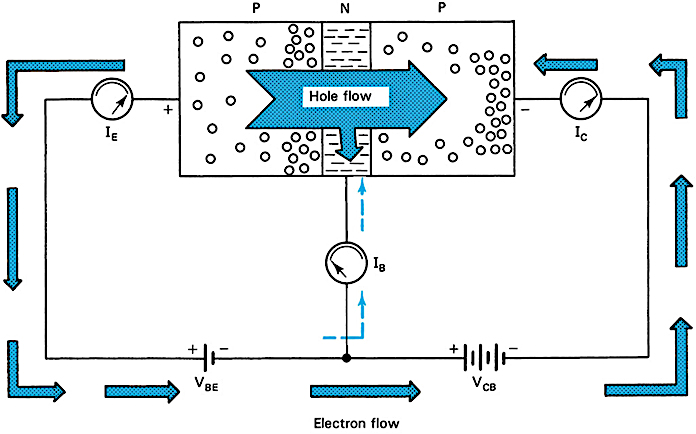
Figure 5. Current carriers of a PNP transistor.
Figure 5 shows how current carriers pass through a properly biased PNP transistor. Forward biasing the emitter base junction causes a large number of holes to move through the junction. On arriving in the base region, a very small number of these holes combine with electrons. This is representative of the base current. Ninety-five percent to ninety-nine percent of the holes move through the base region and enter the collector junction. These holes do not find electrons to combine with in the thin base region. They are, however, immediately influenced by the negative $V_{CB}$ voltage of the collector. This action causes the hole current to flow through the reverse- biased, base collector junction.
The end result is IC passing through the collector region. It then leaves the collector and flows into $V_{CB}$, $V_{BE}$, and returns to the emitter. The large arrow inside the transistor indicates hole current flow. Outside the transistor, electrons achieve current flow. Smaller arrows in the diagram show the current outside the transistor.
Comparison of NPN and PNP Transistor Biasing
Compare the transistors of Figure 4 and Figure 5, and note the polarity of $V_{CB}$ and $V_{BE}$. The polarity shows the primary difference in NPN and PNP transistor biasing. Note also the type of majority current flow through each transistor. This is represented by the large arrow of each diagram. It is different for each device. This means that the two transistor types are not directly interchangeable. Substituting one for the other would necessitate a complete reversal of bias voltage.
PNP transistors are not as widely used as NPN transistors. Electron current flow of the NPN device has much better mobility than the hole flow of a PNP device. This means that electrons have a tendency to move more quickly through the crystal material than holes. Because of this characteristic, NPN transistors tend to respond better at high frequencies. In general, this means that the NPN device has a wider range of applications. Manufacturers usually have a larger selection of these transistors in their lines. With a better selection of transistors available, circuit designers find it easier to select devices of a desired characteristic. As a result, the NPN device is much more popular than its PNP counterpart.
Review Questions
Answer the following questions.
- The emitter-base junction of an NPN transistor must be ________ biased for proper operation.
- The base-collector junction must be ________ biased in an NPN transistor.
- In a typical transistor circuit, base current is approximately ________ to ________ of the emitter current.
- Most of the emitter current in a properly biased transistor passes into the ________.
- The relationship between emitter current, base current, and collector current is expressed as ________.
Answers
- Forward
- Reverse
- 1$\%$ to 5$\%$
- Collector
- $I_{E}=I_{B}+I_{C}$
Key Takeaways
Proper transistor operation requires forward biasing the emitter-base junction and reverse biasing the collector-base junction. In NPN transistors, most emitter current becomes collector current, with minimal base current due to the thin, lightly doped base. PNP transistors operate similarly but with reversed polarities and hole-based current flow. However, NPN devices are favored for their faster electron mobility, better high-frequency performance, and broader availability.