The working of a transistor is like a gated device to the electric current. If the gate is open, there is a flow, and if the gate is closed, there is no flow. The role of the transistor input signal is to open and close the gate, as desired. The output is, thus, controlled by the input.
When the gate is open, energy is delivered to the output (e.g., to a load). From the power viewpoint, the important fact in the operation of a transistor is that the input power is much smaller than the output power.
Figure 1 shows a transistor circuit. The collector is connected to the positive side of a 12 V battery through a resistor R2, and the emitter to the negative side.
At the same time, a smaller (1.5 V) battery is connected between the base and the emitter through the resistor R1 and a switch. The polarity of this battery is such that the base-emitter junction is forward biased, that is, the positive side to the base.
In this sense, there are two loops formed for the electric flow, one between the collector and the emitter, and one between the emitter and the base (emitter is the common terminal).
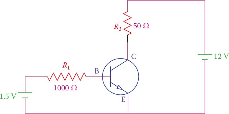
Figure 1 Connecting a transistor to electric supply.
While the collector-emitter loop is closed (and there is no switch), no current flows from the collector (positive side) to the emitter. Also, in the base-emitter circuit, there is no current when the switch is open.
Now, if the switch is closed, a small current of 0.8 mA (that is, [1.5 V − 0.7 V]/1000 Ω, assuming a silicon-based transistor) can flow through R1 from base to the emitter. This current from the base to emitter can cause conduction in the transistor between the collector and the emitter (the second loop). Its function is, in fact, similar to opening a gate, as a result of which a current of around 240 mA (i.e., 12 V/50 Ω) flows from the collector to the emitter. In other words, closing the switch in the first loop causes a current in the second loop.
Consider now the power in the two loops, by multiplying the loop current and its voltage. It is evident that the power in the second loop (12 V × 0.240 A = 2.88 W) is much greater than that of the first loop (1.5 V × 0.0008 A = 0.00120 W).
The above explanation shows the way a transistor works. That is to say, the functioning of a transistor is based on currents in the two loops and not the voltages. This implies that a transistor is a current driven device.
Note that in this simple analysis we have ignored the internal resistances in the junctions between the three elements (base, collector, and emitter) of a transistor.
In reality, there is always some resistance between these elements. It is also imperative to note that the transistor, itself, does not generate power. All the power necessary for amplification comes from the battery (the power supply).
When there is no current between the base and the emitter in a transistor, the transistor is off. When a current flows between the base and the emitter, a current also flows between the collector and the emitter.
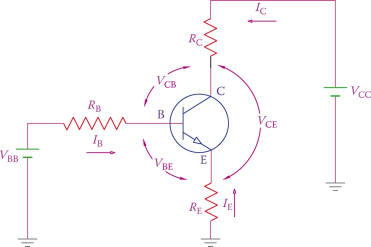
Figure 2 Definition of voltages and currents in a transistor.
Transistor Properties
Figure 2 depicts the definitions for various voltages and currents in a transistor.
- The voltage between the base and the emitter is denoted by VBE.
- The voltage between the collector and the emitter is denoted by VCE, and similarly, the voltage between the collector and the base is denoted by VCB.
- Likewise, the currents flowing through the base, the collector and the emitter are, respectively, represented by IB, IC, and IE.
- Moreover, as indicated in Figure 2, the total voltage supplying power to the collector is called VCC and that corresponding to the base is called VBB.
- By the same token in other transistor configurations, a supply voltage may be used for the emitter. In such a case this voltage is represented by VEE.
If VBE, is less than 0.7 V (assuming a silicon transistor), no matter how much the voltage between the collector and the emitter is (provided that it is within the rating of the transistor and does not cause a breakdown), no current flows from collector to the emitter. In such a case the transistor is said to be in the cutoff state.
Cutoff: Status of a transistor when it is not operating because of very low (negligible) current.
As soon as VBE becomes larger than 0.7 V, a current (IB) flows from B to E. This is the current through the base. This current turns the transistor on and causes conduction between the collector and the emitter. Thus, the current IC flows through the collector toward the emitter. The current in the emitter, IE, is the sum of IB and IC.
The current in the emitter is the sum of the current in the base and the current in the collector.
It is important to understand the operational characteristics of a transistor. In addition to the fact that it behaves as a gated device, we must also know that a transistor behaves like a variable resistor. This is concerning the voltage VCE and the current from the collector to the emitter (IC).
When a transistor is conducting, the current flow from the collector to the emitter is the major component of interest. This is the output current. There is a voltage drop between the collector and the emitter when this current exists.
Nevertheless, this voltage drop cannot be determined based on the assumption that there is a constant resistance between the collector and emitter terminals inside the transistor. The value of such a resistance is not constant.
A transistor behaves like a variable resistor as far as the relationship between the collector-emitter voltage and the collector current is concerned.
As has been shown in Figure 1, a noticeable characteristic of a transistor is that IC is much larger than IB (it can be 100× or 200× larger).
Moreover, the ratio IC/IB, which is almost constant for a transistor in a given circuit, is denoted by the Greek letter β (beta) and can be used for calculation of IC when IB is known, or vice versa.
β depends on the particulars of a circuit, transistor properties, and temperature (by particulars of a circuit we mean the components, their values, and the circuit arrangement).
The minimum and maximum values for parameters of a transistor are normally given in its datasheet.
$\begin{matrix} {{I}_{C}}=\beta {{I}_{B}} & {} & \left( 1 \right) \\\end{matrix}$
Moreover, because β is normally large (typically, 50 < β < 300), then
$\begin{matrix} {{I}_{E}}={{I}_{B}}+{{I}_{C}}=\beta {{I}_{B}}+{{I}_{B}}=\left( \beta +1 \right){{I}_{B}}\approx \beta {{I}_{B}}={{I}_{C}} & {} & \left( 2 \right) \\\end{matrix}$
Equation 2 implies that, for simplification, in many calculations, IB is set equal to IC.
Note that the electrical values must match with reality; in practice, there are always maximum values for current and power that a device can handle, based on its internal structure and rating.
In other words, one cannot rely only on mathematical relationships for a device that is bound by its physical properties, thus exhibiting limit values for current, voltage, and power that it can handle.
Transistor Example 1
Consider the transistor in the circuit of Figure 1. If the value of β for this transistor is 100 and RC = 50 Ω, what is the voltage VCE?
Solution
The base current is
${{I}_{B}}=\left( 1.5-0.7 \right)\div 1000=0.0008A$
The collector current is β times (100×) the base current
${{I}_{C}}=100*0.0008=0.08A=80mA$
and the voltage drop in RC is
${{V}_{RC}}=50*0.080=4V$
VCE is the difference between the power supply voltage and the voltage drop in RC
${{V}_{CE}}=12-4=8V$
Transistor Example 2
For the transistor in Example 1, what is the internal resistance between the collector and the emitter for the given condition?
Solution
On the basis of the voltage VCE = 8 V and the current IC = 0.08 A, the internal resistance between the collector and the emitter is
$8\div 0.080=100\Omega $
Note that this resistance value is not constant, and changes for other operating conditions.
Transistor Example 3
If in the circuit of Example 1, the resistance RC is substituted by a 200 Ω resistor, what will be the voltage VCE?
Solution
For this case, it can be seen that the voltage drop in RC is 16 V (200 × 0.08). This is greater than the total VCC voltage (12 V), which is impossible. This reflects a bad design, in which the transistor cannot function correctly, or as expected. The voltage drop in RC cannot exceed 12 V.
Transistor Key Takeaways
The working of a transistor as a current-driven, gate-like device is fundamental to its wide range of practical applications. Its ability to control large output currents with small input currents allows it to function efficiently as both a switch and an amplifier. This makes transistors essential in countless electronic devices—from signal processing in communication systems to power regulation in computers and industrial machinery. Their versatility and efficiency, combined with their ability to handle varying resistances and adapt to circuit conditions, make transistors indispensable components in the design and operation of modern electronic circuits.