The article provides an overview of electronic oscillator, explaining their definition, purpose, and basic working principles, including feedback and frequency generation. It also describes various types of oscillators, such as Armstrong, Hartley, Colpitts, crystal-controlled, power, and operational amplifier-based oscillators, highlighting their circuit designs and applications.
Definition: An oscillator is an electronic circuit that generates an ac signal at the desired frequency. An oscillator circuit is usually made up of a wave-producing circuit, amplifier, and feedback circuit. Variations in oscillator design are usually found in the feedback circuit. An oscillator is essential in many electronic applications.
The swinging pendulum can be thought of as an oscillator, Figure 1.
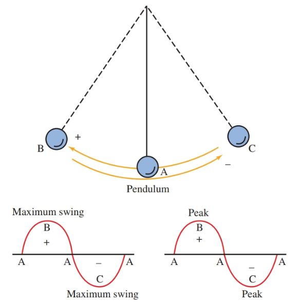
Figure 1. Notice the similarities between the clock pendulum and the oscillating current.
The oscillator is the very heart of radio transmission, microwave communications, radar, and much more.
An oscillating current is one that flows back and forth. It moves first in one direction and then the other. You can compare the oscillator circuit output to a typical ac sine wave. The oscillator circuit changes dc from a power supply input into an ac waveform. The ac waveform maintains a steady frequency using a feedback circuit.
Follow the voltage amplitude in Figure 1. It starts from its reference line and rises to its peak in one direction and then falls to zero. Then it rises to its peak in the opposite direction and returns to zero. One cycle, a complete set of events in a repeated series, has been completed.
As oscillation continues, it repeats this cycle. The time that passes during one cycle is called the period of the cycle. The number of cycles occurring per second is measured and given as the frequency in Hertz.
We learned earlier that the electricity used in homes and factories is an alternating, or oscillating, current. In the U.S. it alternates at a frequency of 60 Hertz. The current is generated by dynamos driven by steam, water, or atomic power.
In our studies of electronics, voltages and currents of much higher frequencies are used. These are generated with semiconductor devices used as oscillators. These devices do not actually oscillate, but they act as valves. These valves feed energy to tuned circuits to maintain the oscillation. The basic block diagram of an oscillator is shown in Figure 2.
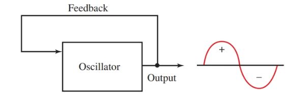
Figure 2. Block diagram of a sine wave oscillator.
Two conditions must exist to sustain oscillation in a tuned circuit:
- The energy fed back to the tuned circuit must be in phase with the first voltage. The oscillator depends upon this regenerative feedback or positive feedback.
- There must be enough feedback voltage amplitude to replace the energy lost by circuit resistance. The principles of the tank circuit operation are an essential part of the timing and feedback portion of many oscillator circuits.
Armstrong Oscillator
An Armstrong oscillator is shown in Figure 3. From this circuit, the basic theory of oscillators can be explained. Notice the tuned tank circuit L1||C1. This determines the frequency of the oscillator. Follow the sequence of events in this circuit.
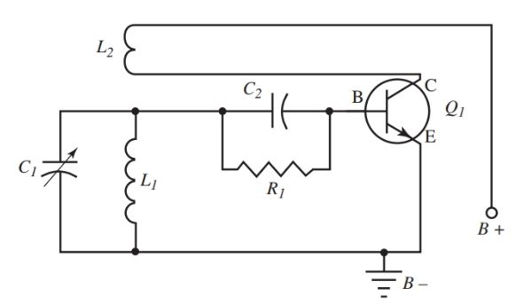
Figure 3. Circuit Diagram of an Armstrong oscillator.
Step 1.
Examine Figure 4. When the voltage is applied to the circuit, current flows from B–, through the transistor and coil L2, to B+. L2 is sometimes called a tickler coil because it provides feedback to L1. L2 is closely coupled to L1.
The expanding magnetic field of L2 makes the base end of L1 positive. C1 charges to the polarity shown. The base of Q1 also collects electrons. It charges C2 in the polarity shown.
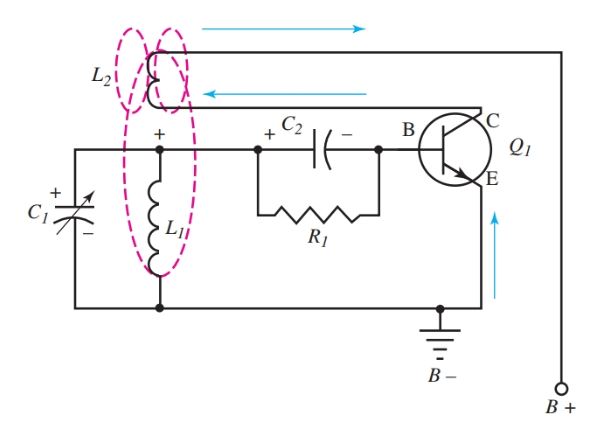
Figure 4. Step 1 in Armstrong oscillator operation. Current flows from B– to B+.
Step2
Examine Figure 5. When Q1 reaches its saturation point, there is no longer a change of current in L2. Magnetic coupling to L1 drops to zero.
The negative charge on the base side of C2 is no longer opposed by the induced voltage of L1. The negative charge drives the transistor to cutoff. This rapid decrease in current through the transistor and L2 causes the base end of L1 to become negative. This increases the negative bias on Q1. C1 discharges through L1 as the first half cycle of oscillation. C2 bleeds off its charge through R1.
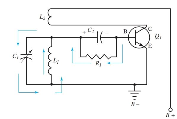
Figure 5. Step 2 in Armstrong oscillator operation. The first half-cycle of oscillation.
Step 3
The transistor, Q1, is held at cutoff until the charge on C2 is bled off to above cutoff. At that time the transistor starts conduction and the cycle is repeated.
There are a few points to remember in Armstrong oscillator operation.
- The voltage developed across L1 first opposes, and then adds to, the bias developed by the R1||C2 combination.
- The energy added to the tuned tank circuit L1||C1 by the tickler coil L2 is great enough to offset the energy lost in the circuit due to resistance. The coupling between L1 and L2 can be adjusted.
- The combination R1||C2 has a somewhat long time constant. It sets the operating bias for the transistor. Q1 is operated Class C.
Study the voltage waveform on the base of Q1 in Figure 6. The shaded portion is transistor conduction. At point B the bias is negative. This results from the charge on C2 plus the induced voltage across L1.
The interval from B to C denotes the time that passes while C discharges through R to the cutoff point, and conduction begins for the next cycle.
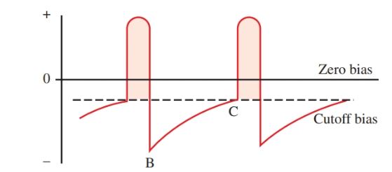
Figure 6. Voltage waveform on the base of the oscillator. Compare it to steps 1, 2, and 3.
Hartley Oscillator
An oscillator used commonly in radio receivers and transmitters is the Hartley oscillator. It is more stable than the Armstrong, but the theory of its operation is similar. The Hartley oscillator is set apart from other oscillators by the tapped coil, L1 and L2 in Figure 7.
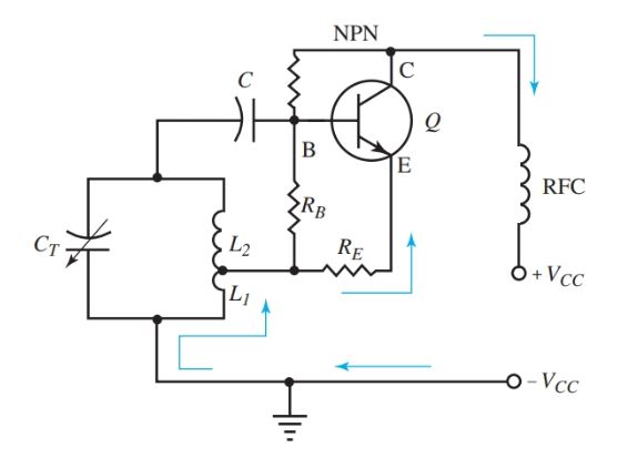
Figure 7. A Hartley oscillator circuit diagram.
- The Hartley parts in Figure 7 are labeled in a manner similar to the labeling used for the Armstrong oscillator in Figures 4 and 5. The L1 section of the coil is in series with the emitter-collector circuit. It carries the total collector current.
- The current IE, which includes IC, is shown by the arrows. When the circuit is turned on, current flow through L1 induces a voltage on L2.
- The voltage induced on L2 makes the base of Q more positive and drives the transistor to saturation. Once the transistor is driven to saturation, the current ceases flowing.
- The magnetic coupling between coils L1 and L2 collapses to zero. The less positive voltage at the base of Q causes the transistor to decrease conduction. This decrease induces a negative voltage at the top end of L2, which is reverse bias for the transistor.
- The transistor is quickly driven to cutoff and the cycle is then repeated. The tank circuit is oscillating, which causes the transistor to switch between saturation and cutoff. The switching action of the transistor is the frequency of the oscillator.
- The resting bias condition of the transistor is set by resistors RB and RE. The radio frequency choke, RFC in the figure, blocks the RF signal from the power source. In this circuit, note that coil L1 is in series with the transistor collector circuit. It is a series-fed oscillator.
In Figure 8, a shunt fed oscillator is shown. The operation is the same. Note that the dc path for the emitter-collector current is not through coil L1. The ac signal path, however, is through C and L1.
At point A, the two current components are separated and required to take parallel paths. Both oscillators receive their feedback energy through magnetic coupling.
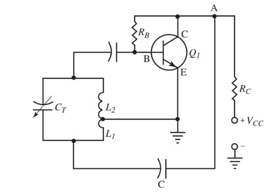
Figure 8. A shunt fed Hartley oscillator circuit diagram.
Other Oscillators
There are quite a number of other types of oscillators you will encounter in the study of electronics. The following section discusses:
- Colpitts oscillators.
- Crystal controlled oscillators.
- Power oscillators.
- Operation amplifier oscillators.
As you study these oscillators, you will notice that they are similar in many ways to the two basic oscillators you have just studied.
Colpitts Oscillator
Feedback can also be created with an electrostatic field such as that found in a capacitor. Replace the tapped coil from the Hartley oscillator with a split stator capacitor. A voltage of proper polarity will be fed back causing the circuit to oscillate. This circuit is called a Colpitts oscillator, Figure 9.
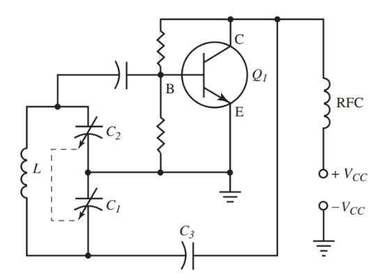
Figure 9. Circuit diagram of a Colpitts oscillator.
- Operation of this oscillator is like that of the Hartley oscillator. However, the signal is coupled back to C1 of the tank circuit through coupling capacitor C3. A changing voltage at the collector appears as a voltage across the tank circuit L||C1C2.
- The tank circuit must be in the proper phase with the transistor circuit to be a regenerative signal. The amount of feedback will depend on the ratio of C1 to C2. This ratio is most often fixed.
- Both capacitors C1 and C2 are controlled by a single shaft (called a ganged capacitor). The frequency of the oscillator is set in a common manner.
- The tuned tank consists of L and C1 and C2 in series. The circuit is shunt fed. Series fed is not possible due to the blocking of dc by the capacitors.
Crystal Controlled Oscillator
A circuit with a stable high frequency is the crystal controlled oscillator. It is used in radio communications, broadcasting stations, and in equipment requiring a fixed frequency with little drift.
As we know that an emf can be made with mechanical pressure and/or distortion of certain crystalline substances. The opposite is also true. A voltage applied to the surface of a crystal will cause distortion in the crystal. These effects are called piezoelectric effects.
When electrical pressure is applied to a crystal, it will oscillate. The frequency of oscillation depends on the size, thickness, and kind of crystal used.
Look at Figure 10. The crystal is precisely cut and mounted on two connection leads using conductive cement. The entire crystal is then enclosed in a metallic can that is filled with dry nitrogen gas.
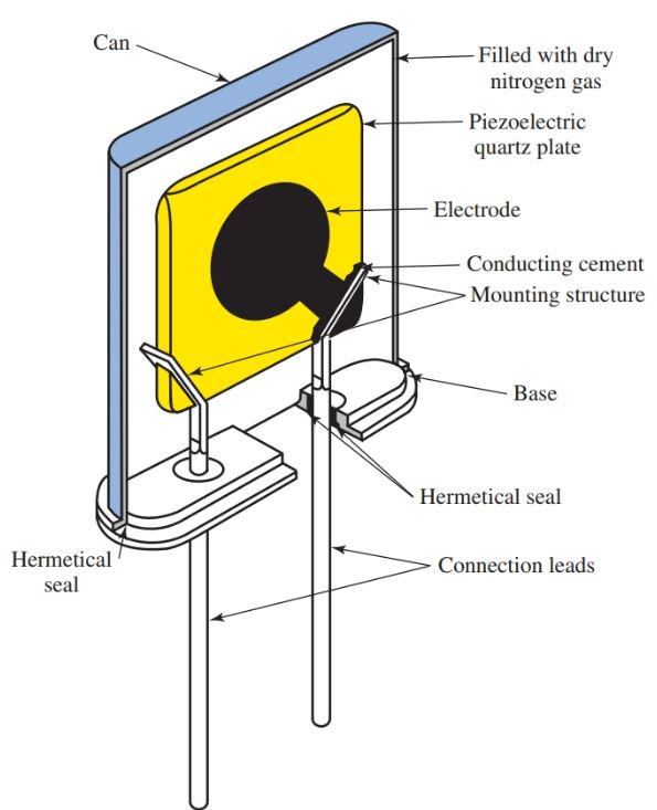
Figure 10. Section of a quartz crystal unit for special and industrial applications.
Figure 11 shows a circuit made of electrical components that are equivalent to a crystal. A crystal is placed between two metallic holders. This forms a capacitor CH. The crystal itself is the dielectric.
CG denotes the series capacitance between the metal holding plates and the air gap between them (as a dielectric). L, C, and R denote the traits of the crystal. Note the likeness of the equivalent crystal circuit to a tuned circuit. Both a tuned circuit and a crystal will have a resonant frequency.
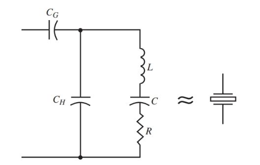
Figure 11. The electrical circuit on the left is roughly equivalent to a piezoelectric crystal (schematic symbol shown at right).
- Crystals are used in amateur radio and commercial broadcasting stations to control the transmitter frequency. The frequency generated by the crystal is susceptible to temperature changes.
- In a commercial broadcasting station, crystals used to control transmitter frequency are placed in crystal ovens. The crystal oven maintains a constant temperature, which will, in turn, stabilize the frequency produced by the crystal.
- A crystal oscillator circuit is shown in Figure 12. Compare this circuit to Figure 8. It is the same circuit with the crystal added to the feedback circuit.
- The crystal acts as a series resonant circuit. It sets the frequency of the feedback currents. The tank circuit must be tuned to this frequency.
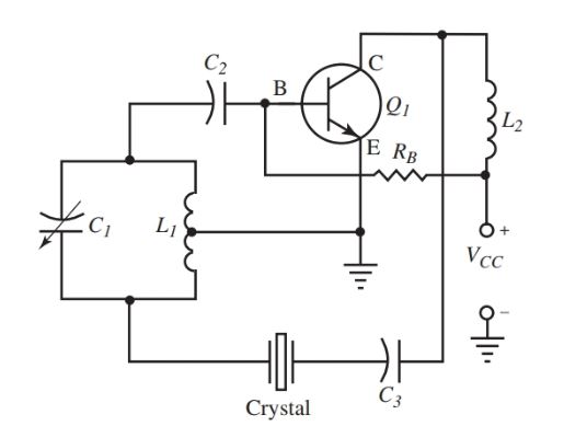
Figure 12. A crystal controlled Hartley oscillator circuit.
In Figure 13, the crystal is used in place of the inductor in the tank circuit of the Colpitts oscillator. This is the Pierce oscillator. Compare the circuit to Figure 9.
The amount of feedback needed to energize the crystal, again, depends on the ratio of C1 to C2. These capacitors form a voltage divider across the emitter-base of the transistor. The Pierce circuit is stable under changing circuit conditions.
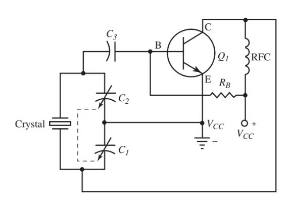
Figure 13. A crystal controlled Pierce oscillator circuit.
Additional uses for crystals
A crystal changing frequency because of a change in temperature is undesirable in an oscillator circuit. However, this trait can be used to our advantage as well.
The frequency developed by a quartz crystal varies in direct proportion to the temperature to which it is exposed.
Figure 14 shows a simple circuit for measuring temperature. Two crystals are used. One crystal is used as a reference, and the other crystal is exposed to the temperature being measured.
The crystals will produce two different frequencies, which are input to the differential counter. The differential counter is a digital integrated circuit.
The two frequencies are compared and then can be displayed on a number of different devices such as analog meter, digital meter, LED display, etc. The accuracy of this system can be up to ±0.001 Kelvin.
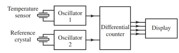
Figure 14. Quartz crystal used for temperature measurement.
Quartz crystals are also used in timing devices because of their stability and accuracy. A signal generator is an electronic oscillator that generates various signals for testing, Figure 15.
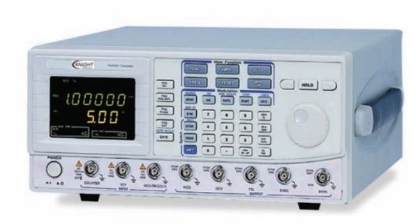
Figure 15. Commercial signal generator. (Knight Electronics, Educational Products Division)
Power Oscillator
Figure 16 shows a power oscillator circuit. This schematic is of a push-pull oscillator. The collector load of each transistor is the primary of the transformer. The ac output is found at the secondary. A proper turns ratio is used if higher or lower voltages are needed.

Figure 16. Power oscillator circuit diagram
- A slight imbalance in conductivity between Q1 and Q2 will start oscillation. This imbalance is always present due to variances in transistor characteristics or temperature. This will send one of the transistors toward saturation and the other toward cutoff.
- Assume Q1 starts conducting. The voltage at C of Q1 goes less positive. This makes the base of Q2 less positive. Q2 drives toward cutoff. A more positive voltage at C of Q2 drives the Q1 base more positive. Q1 reaches saturation.
- When there is no change in current at saturation, transformer primary reactance drops to zero. Collector voltage toward the value of VCC also increases. This more positive voltage coupled to the base of Q2 through R1 starts Q2 toward conduction and saturation.
- The transistors conduct one at a time. The output is combined into a complete cycle at the transformer secondary output.
- If the output from the transformer in Figure 16 is connected to a rectifier and some filter circuits, the output again becomes dc.
Operational Amplifier Oscillator Circuit
The operational amplifier can be used in many oscillator circuits in place of a transistor in such circuits as the Hartley or Colpitts oscillator. See Figure 17.
Notice that the crystal is used in the feedback circuit of the op-amp. The charging circuit—R1, R2, and the capacitor—determine the amount of feedback and wave shaping. The NAND gate is used to start the output from the op-amp. Without it, the circuit would need some exterior input to start the circuit.
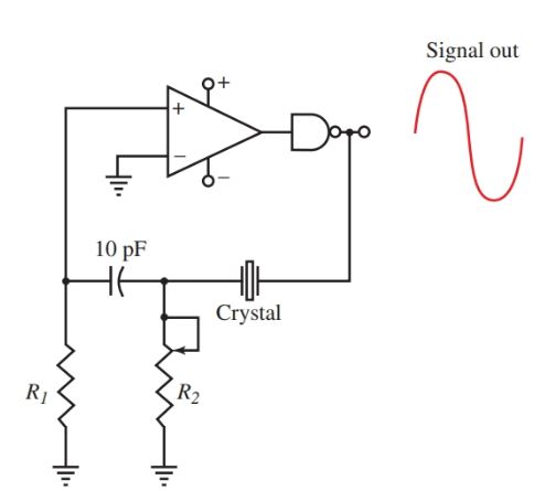
Figure 17. Crystal oscillator using an op-amp.
Another oscillator that can utilize the op-amp is the Wien bridge oscillator. See Figure 18. This circuit operates using both positive and negative feedback.
The negative and positive feedback circuits must be balanced for the oscillator to work properly. The balancing is achieved by inserting the tungsten filament lamp in the circuit as part of the feedback system.
The resistance of the lamp varies with the amount of current in the lamp filament. As current increases, the temperature of the filament increases and so, too, the resistance value of the filament. The inverse is also true. As current decreases, temperature decreases and in turn the resistance value of the filament also decreases. This principle is the secret to balancing the amount of feedback in the circuit.
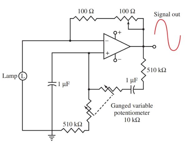
Figure 18. The Wien bridge oscillator circuit diagram
Many types of oscillators are formed on a single linear integrated chip. Only a few extra components are needed to produce a working oscillator. Some are voltage controlled oscillators (VCO), Figure 19.
The frequency output of the oscillator is in direct proportion to the voltage level applied to one of the VCO’s pins.
Figure 19. A general purpose voltage controlled oscillator (VCO) function generator. This chip can be used as a voltage controlled oscillator or as the wave shaping device for a function generator.
Oscillator Key Takeaways
Oscillators play a crucial role in modern electronics by generating stable and precise alternating current (AC) signals, which are fundamental to countless applications. They are essential in radio transmissions, microwave communications, radar systems, and signal generation for testing and measurement. Crystal-controlled oscillators ensure frequency stability in broadcasting and telecommunications, while power oscillators enable efficient energy conversion in various circuits. Additionally, operational amplifier-based and voltage-controlled oscillators (VCOs) provide flexibility in waveform generation for advanced electronic systems.