This article explores the three main transistor circuit configurations: common-emitter, common-base, and common-collector, detailing their operating principles, gain characteristics, and applications in amplifying signals.
The circuit configurations of bipolar transistor amplifiers describe the various ways a BJT can be integrated into an amplifier circuit to achieve specific amplification characteristics. The elements of a transistor can be connected in one of three different circuit configurations. These are usually described as common-emitter, common-base, and common-collector.
Of the three transistor leads, one is connected to the input and one to the output. The third lead is commonly connected to both the input and output. The common lead is generally used as a reference point for the circuit. It is usually connected to the circuit ground or common point. This has brought about the terms grounded emitter, grounded base, and grounded collector. The terms common and ground mean the same thing in the field of electronics.
In some circuit configurations, the emitter, base, or collector may be connected directly to the ground. When this occurs, the lead is at both DC and AC ground potential. When the lead goes to ground through a battery or resistor that is bypassed by a capacitor, it is now considered to be at an AC ground only. The capacitor provides a low impedance path for the amplified AC signal but blocks the DC component. With no bypass capacitor, the emitter bias voltage and, thus, the operating point of the transistor fluctuate at the frequency of the amplified signal, causing distortions.
Common-Emitter Amplifier
The common-emitter amplifier is a very important amplifier circuit. A very high percentage of all amplifiers in use are of the common-emitter type. The input signal of this amplifier is applied to the base, and the output is taken from the collector. The emitter is the common or grounded element. Figure 1 shows a circuit diagram of the common-emitter amplifier.
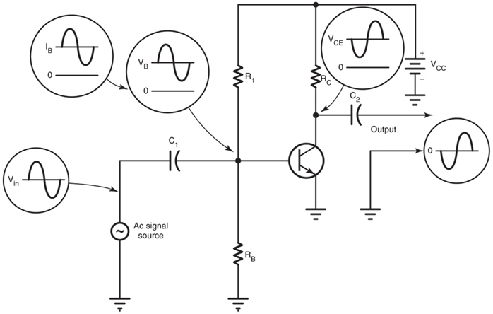
Figure 1. Circuit diagram of a common-emitter amplifier.
The signal amplified by the common-emitter amplifier is applied to the emitter-base junction. This signal is superimposed on the DC bias of the emitter-base. The base current then varies at an AC rate. This action causes a corresponding change in collector current. The output voltage developed across the collector-emitter is inverted $180^\circ$.
The current gain of the circuit is determined by the $\beta$. Typical $\beta$ values are about $50$. Voltage gain ranges from $250$ to $500$. Power gain is about $2000$. Input impedance is moderately high, typically around $100 \ \Omega$. Output impedance is moderate; a typical value is about $2 \ k\Omega$.
Remember that impedance is the opposition to alternating current, in this case, at the input and output terminals of the device. In general, common-emitter amplifiers are used in small-signal applications or as voltage amplifiers.
Common-Base Amplifier
A common-base amplifier is shown in Figure 2. In this type of amplifier, the emitter-base junction is forward-biased, and the collector-base junction is reverse-biased. The emitter is the input. An applied input signal changes the circuit value of $I_{E}$. The output signal is developed across $R_{L}$ by changes in collector current. For each value change in $I_{E}$, there is a corresponding change in $I_{C}$. In a common-base amplifier, the current gain is called alpha ($\alpha$). Alpha is determined by the following formula:
$$\alpha = \frac{I_{C}}{I_{E}}$$
The value of the gain in a common-base amplifier is always less than 1. Now, recall that:
$$I_{E} = I_{B} + I_{C}$$
The $I_{C}$ will, therefore, always be slightly less than $I_{E}$ by the value of $I_{B}$. $I_{E}$ is the signal input but is the source input for $I_{B}$ and $I_{C}$. Typical values of alpha are 0.98−0.99.
In Figure 2, $V_{EE}$ forward biases the emitter-base, whereas $V_{CC}$ reverse biases the collector-base. Resistor $R_{E}$ is an emitter current-limiting resistor, and $R_{L}$ is the load resistor. Note that the transistor is a PNP type.
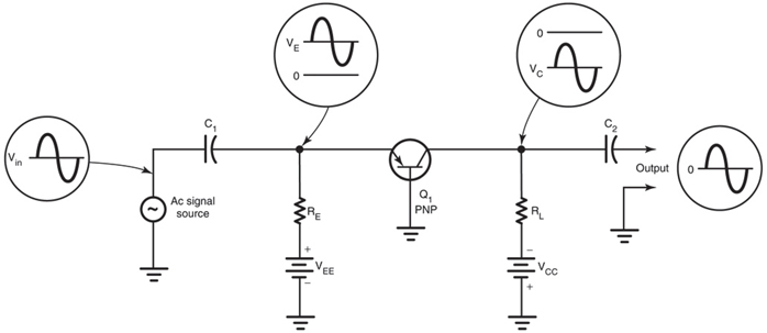
Figure 2. Circuit diagram of a common-base amplifier.
When an AC signal is applied to the input, it is added to the DC operating value of $V_{E}$. The positive alternation, therefore, adds to the forward-bias voltage of $V_{E}$. This condition causes an increase in $I_{E}$. A corresponding increase in $I_{C}$ also takes place. With more $I_{C}$ through $R_{L}$, there is an increase in its voltage drop. The collector, therefore, becomes less negative, or swings positive. In effect, the positive alternation of the input produces a positive alternation in the output. The input and output of this amplifier are in phase. See the waveform inserts in the diagram. The negative alternation causes the same reaction, the only difference being a reverse in polarity.
A common-base amplifier has a number of unique characteristics that should be considered when this amplifier is selected for an application. Its current gain is called alpha. The current gain is always less than 1. Typical values are $0.98$ and $0.99$. Voltage gain is usually very high. Typical values range from $100$ to $2500$ depending on the value of $R_{L}$. Power gain is the same as voltage gain. The input impedance is very low. Values of $10$–$200 \ \Omega$ are very common. The output impedance of the amplifier is somewhat moderate. Values range from $10 \quad$ to $\quad 40 \ k\Omega$. This amplifier does not invert the applied signal.
Common-base amplifiers are used primarily to match a low-impedance input device to a circuit. This type of circuit configuration is used in radio-frequency amplifier applications. As a general rule, the common-base amplifier is not used very commonly.
Common-Collector Amplifier
A common-collector amplifier is shown in Figure 3. In this circuit, the base serves as the signal input point. The input of this amplifier is primarily the same as the common-emitter circuit. The collector is connected to ground through $V_{CC}$. Note that the input, output, and collector are all commonly connected. The unique part of this circuit is the output. It is developed across the load resistor ($R_{L}$) in the emitter. There is no resistor in the collector circuit.
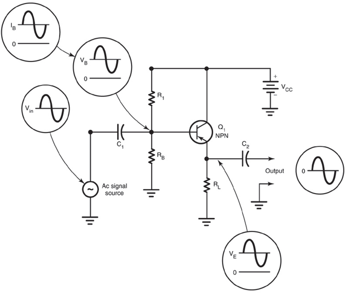
Figure 3. Common-Collector Amplifier Circuit Diagram
When an AC signal is applied to the input, it adds to the base current. The positive alternation increases the value of $I_{B}$ above its static operating point. An increase in $I_{B}$ causes a corresponding increase in $I_{E}$ and $I_{C}$. With an increase in $I_{E}$, there is more voltage drop across $R_{L}$. The topside of $R_{L}$ and the emitter become more positive. A positive input alternation, therefore, causes a positive output alternation across $R_{L}$. Essentially, this means that the input and output are in phase. The negative alternation reduces $I_{B}$, $I_{E}$, and $I_{C}$. With less $I_{E}$ through $R_{L}$, the output swings negative. The output is again in phase for this alternation.
The common-collector amplifier is capable of current gain. A small change in $I_{B}$ causes a large change in $I_{E}$. This current gain does not have a descriptive term such as alpha or beta. In general, the current gain is assumed to be greater than 1. Values approximate those of the common-emitter amplifier.
Other factors of importance are voltage gain, power gain, input impedance, and output impedance. Voltage gain is less than 1. Power gain is moderately high, with typical values in the range of $50$. Input impedance is in the range of $50 \ k\Omega$. The output impedance is quite low because of the location of $R_{L}$. Typical values are about $50 \ \Omega$.
Common-collector amplifiers are used primarily as impedance-matching devices. They can match a high-impedance device to a low-impedance load. Practical applications include preamplifiers operated from a high-impedance microphone or phonograph pickup. Common-collector amplifiers are also used as driver transistors for the last stage of amplification. In this application, power transistors generally require large amounts of input current to deliver maximum power to the load device. Since the emitter output follows the base, this type of amplifier is often called an emitter follower.
Comparing Three Transistor Amplifier Configurations
Here is a concise comparison table showing the key differences between the three basic Transistor amplifier configurations — Common Emitter (CE), Common Base (CB), and Common Collector (CC):
| Parameter | Common Emitter (CE) | Common Base (CB) | Common Collector (CC) |
| Configuration | Base is common to both input and output | Emitter is input, collector is output; base common | Collector is common to both input and output |
| Input Signal Applied To | Base | Emitter | Base |
| Output Taken From | Collector | Collector | Emitter |
| Input Impedance (Z₁) | Moderate (1 kΩ – 5 kΩ) | Very low (tens of Ω) | High (hundreds kΩ) |
| Output Impedance (Z₀) | Moderate to high | High | Very low |
| Current Gain (β or α) | High (≈ β ≈ 20 – 500) | Less than 1 (≈ α ≈ 0.95 – 0.99) | High (≈ β + 1) |
| Voltage Gain (Aᵥ) | High (≈ 100 – 500) | High (≈ 50 – 500) | < 1 (voltage follower) |
| Power Gain (Aₚ) | Very high | Moderate | Moderate |
| Phase Relationship | Output is 180° out of phase with input | Output is in phase with input | Output is in phase with input |
| Bandwidth | Moderate | Highest among the three | Moderate to low |
| Applications | General-purpose amplification, audio amplifiers | RF amplifiers, impedance matching | Buffering, impedance matching, voltage follower |
| Key Advantage | High voltage and power gain | Excellent high-frequency response | High input and low output impedance (ideal buffer) |
| Key Limitation | Moderate frequency response; phase inversion | Low input impedance | Voltage gain less than unity |
Review Questions
- The input of a common-emitter amplifier is connected to the __________.
- The output of a common-emitter amplifier is connected to the __________.
- The input and output of a common-emitter amplifier are __________ out of phase.
- The current gain of a common-emitter amplifier is determined by the transistor’s __________.
- The input signal of a common-base amplifier is applied to the __________, and the output is removed from the __________.
- The input and output of a common-base amplifier are __________ phase.
- The current gain of a common-base amplifier is called __________.
- The current gain of a common-base amplifier is always __________ than 1.
- The input of a common-collector amplifier is applied to the __________, and the output is derived from the __________.
- The input and output of a common-collector amplifier are __________ phase.
- The voltage gain of a common-collector amplifier is __________ than 1.
Answers
- Base
- Collector
- Out
- Beta
- Emitter, Collector
- In
- Alpha
- Less
- Base, Emitter
- In
- Less
Key Takeaways
Transistor circuit configurations—common-emitter, common-base, and common-collector—are crucial for amplifying signals in various electronic applications. Understanding their specific characteristics, such as current gain, voltage gain, and impedance, allows engineers to select the appropriate amplifier for different scenarios, from small-signal amplification to impedance matching. These configurations find wide applications in audio amplification, radio-frequency applications, and as driver stages in power circuits.