This article discusses the basic construction methods used to manufacture bipolar junction transistors (BJTs), focusing on alloy-junction and diffusion techniques, and highlights the different types of transistor packaging available.
BJT Construction Methods
Since the invention of the first transistor, a variety of construction methods have been used to manufacture this device. The first transistors manufactured were of the point-contact type. In this method, semiconductor materials are connected together by pointed wires that are fused to the material. For many years, transistors constructed by this method were primarily used in high-frequency applications. Other manufacturing methods are alloy-junction and diffusion. This article briefly discusses the alloy-junction and diffusion methods.
Alloy-Junction Transistors
The alloy-junction method of bipolar transistor construction is an outgrowth of a procedure that is used to form diodes. In transistor construction, this procedure is achieved by attaching two small pieces of metal on opposite sides of a thin piece of semiconductor material. The metal pieces serve as an impurity or dopant for the semiconductor.
Figure 1 shows a structure with this formation. The entire structure is then heated until the impurity melts into the semiconductor material. The melting process causes an alloy of a different type to be formed on each side of the semiconductor. In this case, a PNP-type device is formed by the alloying procedure.
The three semiconductor materials formed by the alloying process represent the emitter, base, and collector of a BJT. Leads are attached to each material. The entire structure is then placed in a housing with the three leads serving as external connection points to the respective material.
Note in Figure 1 that the collector base area of the transistor is made larger than the emitter base area. This is purposely done to permit the collector to have greater power dissipation. The alloy-junction technique of transistor fabrication has been used in the manufacture of high-power transistors.
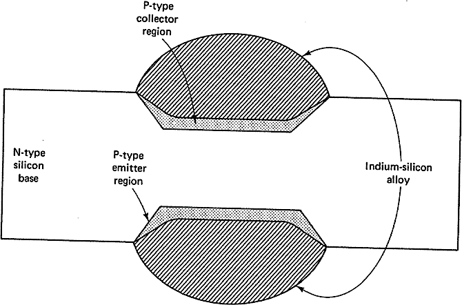
Figure 1. PNP alloy-junction transistor formation.
Diffusion Transistors
Bipolar junction transistors are largely manufactured by the diffusion technique. This process involves the movement of N-type or P-type impurity atoms into a piece of silicon. To achieve this movement, it is necessary to heat a piece of silicon to 1250°C in the presence of a controlled impurity vapor. The movement process is very slow. Typical formation rates are 0.00001 inch per hour.
The diffusion process is carried out in two steps. The first step consists of heating a piece of silicon in an impurity dopant vapor to form a high concentration of the dopant on its surface. This is called the deposition step. The silicon piece then has its temperature elevated. This causes the dopant atoms to be absorbed or diffused into the silicon. This is called the diffusion step. Manufacturing involves repeated deposition and diffusion steps.
Figure 2 shows transistor formation by the diffusion process. The first step involves an N-type semiconductor that has a P-type vapor deposited on its surface. In the second step, increased heat causes the P-type material to diffuse into the N-type material. This forms an N-type collector and a P-type base. The third step is a repeat of the initial process. In it, however, the dopant vapor is a pentavalent material. The deposition area is on top of the base. This causes an area of N-type material to be formed on the base. Diffusion causes this material to move into the base. The structure now has an N-type emitter. The completed transistor is an NPN device.
A refined version of the diffusion process is called epitaxial growth. In this fabrication technique, N-type or P-type materials are grown or formed on the surface of another material. The general shape of specific transistor elements can be altered through this procedure. The term epitaxial is derived from the Greek words epi, meaning on, and taxi, meaning arrange. This describes the process in which atoms are formed on a surface so that they are an extension of the original crystal structure.
When the epitaxial growth process is used and the completed structure has a flat top or level plane surface, the transistor is called a planar transistor. When the completed structure rises above the primary surface, forming a plateau, it is called a mesa transistor. Mesa construction is used to expose the emitter and base regions so that electrical connections can easily be made.
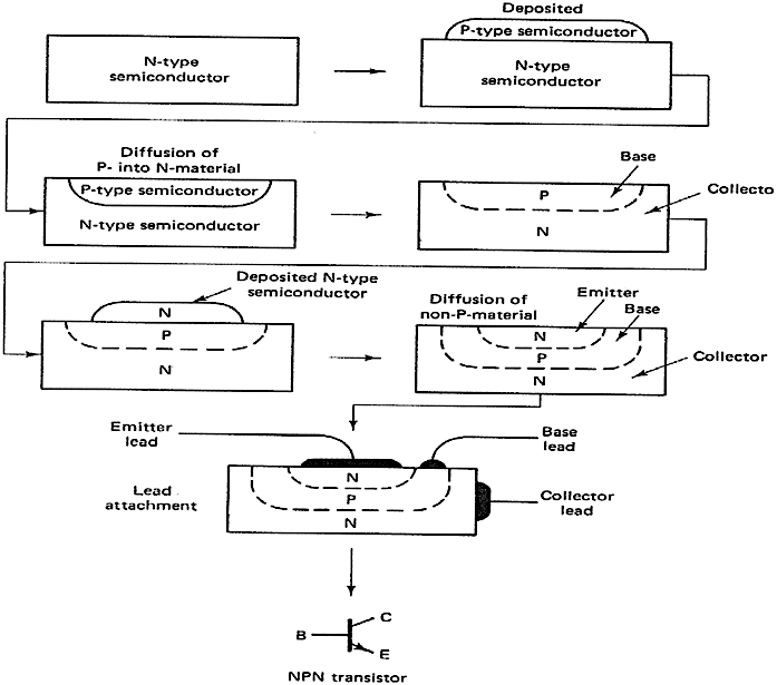
Figure 2. Transistor formed by the diffusion process.
Packaging Techniques for BJTs
Once a transistor is constructed, the entire crystal assembly must be placed in an enclosure or package. The unit is then sealed to protect it from dust, moisture, or outside contaminants. Electrical connections are made to each element through leads attached to the package.
When metal packages are used, the housing also serves as a heat sink, which carries heat away from the crystal. A common practice with this kind of unit is to attach the collector to the metal case. This helps the collector dissipate heat. Packages of this type should not be permitted to touch other circuit components when they are in operation.
Ceramic- and epoxy-packaged transistors are also available. As a rule, this type of packaging is somewhat less expensive than metal packaging to produce. However, these devices are usually not as rugged as the metal-packaged devices. Most small-signal transistors are housed in epoxy packages. The outside case of this device is insulated from all transistor elements. It is specifically designed for printed circuit board construction and close placement with other circuit components.
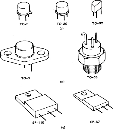
Figure 3. Typical transistor packages. (a) Small-signal. (b) Large-signal or power. (c) Epoxy.
Several transistor package styles are shown in Figure 3. Figure 3(a) shows devices designed for small-signal applications. The letter designation “TO” stands for transistor outline. These same packages are also used to house other solid-state devices.
Figure 3(b) shows some of the packages used to house large-signal or power transistors. Heavy metal cases of this type are used to dissipate heat generated by the transistor. The collector is usually attached to the metal case.
Figure 3(c) shows a few of the common epoxy packages. The letter designation “SP” stands for semiconductor package. This type of package is used to house a number of other semiconductor devices.
With the wide range of package styles available, it is difficult to have a standard method of identifying transistor leads. Each package generally has a unique lead location arrangement. It is usually a good idea to consult the manufacturer’s specifications for proper lead identification.
Review Questions
- The _______ transistors are formed by melting two small metal pieces into opposite sides of a thin piece of semiconductor material.
- The _______ takes place when a thin layer of dopant material is formed on the surface of silicon.
- The _______ occurs when a concentration of dopant material is absorbed into a piece of silicon.
- A fabrication procedure that causes a flat surface structure to be formed produces a _______ transistor.
- A fabrication procedure that causes a plateau area to rise on the surface of a structure produces a(n) _______ transistor.
- The letter designation “TO” stands for _______.
- The letter designation “SP” stands for _______.
Answers
- Alloy-junction
- Deposition
- Diffusion
- Planar
- Mesa
- Transistor Outline
- Semiconductor Package
Key Takeaways
Transistors are constructed using techniques like alloy-junction and diffusion, where impurities are introduced into silicon to form the desired semiconductor layers. Epitaxial growth further refines this process, enabling the creation of planar and mesa structures. Once the transistor is fabricated, it is enclosed in metal, ceramic, or epoxy packages that not only protect the internal components but also help manage heat dissipation. Metal packages, in particular, aid in thermal management by connecting the collector to the case, improving overall performance. Since different packaging styles affect lead identification, it’s essential to consult the manufacturer’s specifications to ensure proper connection.