The article provides an overview of diodes, explaining their construction, working principle, and behavior under forward and reverse bias configurations. It highlights the role of the PN junction, the impact of material properties, and the key characteristics and symbols associated with diodes.
What is a Diode?
A diode is the simplest semiconductor device made of a single PN junction, allowing current to flow in one direction while blocking it in the opposite direction. It is widely used in electronic circuits for rectification, protection, and signal processing.
Diode Working Principle
Its function is to let electric current flow in one direction but to prevent flow in the opposite direction. This is a very important and useful property. This function is similar to a check valve in hydraulics.
The check valve depicted in Figure 1a opens when the pressure in the left side of the pipe is greater than that in the right-hand side, but it prevents any fluid going from the right side to the left. The applications of a check valve are plenty; for instance, at the entrance of the pipe in a well connected to a pump, a check valve is used in order to prevent water from flowing back to the well (Figure 1b).
Also, to protect a pump from being under high pressure when not working, a check valve can be installed at its outlet.
Similarly, in electronic circuits, diodes can be used for protection of a device against a reverse current in case that there is such a possibility.
A diode makes a short circuit across a device an easier path for the current. A more common application of a diode is in rectifiers.

Figure 1 Check valve allowing flow only in one direction. (a) If the pressure on the right exceeds the pressure on the left, the valve closes. (b) If a pump sending water up stops, water is prevented from going back.
A diode is the simplest semiconductor component.
Diode Construction
A PN junction is formed when an N-type material and a P-type material are joined together. This is a through the process in the manufacturing of semiconductor materials, which must be carried out in a very clean environment, called the clean room.
Figure 2 shows an N-type and a P-type material put together. A PN junction is not a physical object that one can buy; it is merely the internal structure of diodes, transistors, and other semiconductor components where a P-type material and an N-type material are joined.
Where the two types of materials contact each other, there is a small boundary where the holes (with a positive charge) attract the electrons (with a negative charge). As the attracted electrons gather near this boundary, their negative charges accumulate and then they repel any additional electron to become attracted by the holes.
Similarly, the holes also gathered on the other side of the boundary, repel any other holes from coming near. The area formed this way is called the depletion region, also depicted in Figure 2.

Figure 2. PN Junction Diode Diagram
Depletion region: Narrow width area in a semiconductor junction just between the N-type and P-type materials.
The flow of electrons and holes to the depletion region continues until they balance each other and a state of equilibrium is reached. In this sense, the depletion region would be thinner or thicker, depending on the amounts of impurities when manufacturing the PN junction.
Notice that in the study of electronics, in the same way, that electric current is considered to be due to the flow of electrons, sometimes the flow of holes is considered, instead. For simplicity, the term carrier is used as the cause of current. A carrier, thus, can be electrons or holes.
Carrier: The entity (either electrons or holes) that the majority of an electric current in a semiconductor device can be attributed to.
For example, if 94% of current is due to the movement of electrons and 6% is due to a hole, then electrons are the carrier.
Forward and Reverse Bias
When a PN junction is connected to DC electricity, there are two possibilities: either the P-type side is connected to the positive and N-type side connected to the negative terminal, or vice versa.
In the first case, shown in Figure 3a, the P side of the PN junction is positive with respect to the N side. This configuration is called forward bias, and the junction is said to be forward biased.
The case that the P side is connected to the negative terminal and the N side connected to the positive terminal is called reverse bias (and the junction is said to be reverse biased).
In general, one side can be more positive (or less negative) with respect to the other side. On the basis of this definition, inside a circuit, any PN junction is connected in either forward bias or reverse bias configuration. This is always the case, and one can determine from the voltage relationships whether any PN junction at any time is forward biased, or reverse biased.
Forward bias: Applying a more positive voltage to the P-type side of a PN-junction than that to the N-type.
Reverse bias: Opposite of forward bias: connecting the P-type side of a PN-junction to a less positive or more negative voltage than the voltage connected to the N-type side.
When a PN junction is forward biased, it conducts because the polarity of the circuit helps a current to flow through the junction (see Figure 4a). But, in general, when a PN junction is in reverse bias, electrons are repelled when approaching the depletion region and the flow of electricity is, thus, blocked, as shown in Figure 4b.
N- and P-type materials can be based on silicon or germanium. Moreover, various dopants can be used for doping. As a result, the characteristics of PN junctions vary based on the materials from which a junction is made.
The proportion of the impurity also has a direct effect on the thickness of the depletion region and thus on the properties of a PN junction and the device using the PN junction.
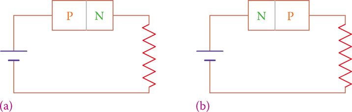
Figure 3. Forward (a) and reverse (b) bias of a PN junction.
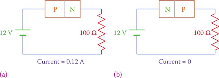
Figure 4. Conduction in a PN junction: (a) forward bias and (b) reverse bias.
Properties of a PN junction depend on the materials and their proportions used in its manufacturing.
Diode Characteristics and Symbol
A diode is the simplest semiconductor device and consists of only one PN junction. It has two wire terminals for connection to the external circuits.
A diode can be connected in a circuit in the forward bias or reverse bias configuration. Figure 5 illustrates the symbol as well as the physical shape of the most common diodes.
The arrow in the symbol shows the direction of the current for the positive toward negative convention. That is the current direction from P side to the N side.
The P side of a diode is called the anode, and the N side is called the cathode. When inside a circuit, for the majority of applications the anode must be connected to the positive terminal (or to a more positive voltage), whereas the cathode is connected to the negative terminal (or to a less positive voltage).
In the physical shape shown in Figure 5, the side denoted by a bar is the cathode. There are other physical shapes for diodes, too, especially for more specific diodes. In practice, the cathode can also be identified by the length of the connection wires. The cathode side connector is always shorter.
Anode: Positive side terminal in a diode and a thyristor.
Cathode: Negative side terminal of a diode or similar devices, as opposed to the anode.
Figure 6 depicts other physical shapes for diodes. The anode and cathode sides are also identified.
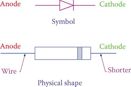
Figure 5 Diode symbol and the most common physical shape.
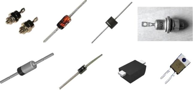
Figure 6. Different shapes of diodes.
For forward bias, the anode must be connected to the positive side (positive terminal or the more positive voltage) in a circuit.
When a diode is inserted in a circuit and is forward biased depending on the material from which the diode is made (silicon or germanium), there is a small voltage drop across the diode. This is due to the resistance to electron flow as a result of the formation of the depletion region. This voltage drop must be brought into consideration in any calculation of current through a diode and its circuit.
For a silicon-based diode this voltage drop is around 0.7 V, and for a germanium-based diode, it is around 0.3 V.
Diode Key Takeaways
Diodes are fundamental components in electronics due to their ability to control the direction of current flow, making them essential for numerous applications. Their use in rectifiers, circuit protection, and signal modulation highlights their versatility and importance in modern technology. The characteristics of diodes, such as the forward voltage drop and behavior under different biases, are crucial for designing efficient and reliable electronic circuits.