Learn the fundamentals of transistor load line analysis through this comprehensive guide, which covers static and dynamic load lines, power dissipation, and the operation of amplifiers.
The graphical method employs a collector family of characteristic curves graph. A load line is developed for this graph and used for load-line analysis. Through load-line analysis, it is possible to predict how the circuit will respond. A great deal about the operation of an amplifier can be observed through this method.
A great deal about the operation of an amplifier can be observed through this method. In this section, you will create a load line for a collector family of characteristic curves graph. You will then use this graph and load line to analyze an amplifier circuit.
The load-line method of circuit analysis is widely used. Engineers use this method in designing new circuits. The operation of a specific circuit can also be visualized by this method. In circuit design, a specific transistor is selected for an amplifier. Source voltage, load resistance, and input signal levels may be given values in the design of the circuit. The transistor is made to fit the limitations of the circuit.
For our application of the load line, assume that the amplifier circuit in Figure 1 is to be analyzed. Note that the power dissipation rating of the transistor is included in the diagram.
Power Dissipation Curve
Maximum power dissipation determines the operational limits of electronic devices. A common practice in load-line analysis for transistors is to first develop a power dissipation curve. This gives some indication of the maximum operating limits of the transistor. Power dissipation ($P_{D}$) refers to the maximum heat that can be given off by the base-collector junction. Usually, this value is rated at 25$^\circ$C. The $P_{D}$ is the product of $I_{C}$ and $V_{CE}$. In our circuit, the $P_{D}$ rating for the transistor is 300 mW.
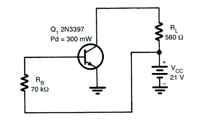
Figure 1. Circuit Diagram of BJT Amplifier.
To develop a $P_{D}$ curve, each value of $V_{CE}$ is used with the $P_{D}$ rating to determine an $I_{C}$ value. The formula is:
$$I_{C}=\frac{P_{D}}{V_{CE}}$$
Using this formula, the $I_{C}$ value is calculated for each of the $V_{CE}$ values of the collector family of curves. Then, the $V_{CE}$ value and the corresponding calculated $I_{C}$ value are located and noted. These points are connected together to form the 300-mW power dissipation curve. In practice, the load line must be located to the left of the established $P_{D}$ curve. Satisfactory operation without excessive heat generation can be assured in that area of the curve.
Example 1
Using the transistor characteristic curve of Figure 2, calculate the values of collector current for a 300-mW power dissipation curve for $V_{CE}$ values of 9 V and 12 V.
Solution
$$I_{C}=\frac{P_{D}}{V_{CE}} $$
At 9 V:
$$I_{C}=\frac{300\ \text{mW}}{9\ \text{V}}=33.33\ \text{mA}$$
At 12 V:
$$I_{C}=\frac{300\ \text{mW}}{12\ \text{V}}=25\ \text{mA} $$
Static Load Line Analysis
The load line of a transistor amplifier represents two extreme conditions of operation. One of these is in the cutoff region. When the transistor is cut off, no $I_{C}$ flows through the device. $V_{CE}$ equals the source voltage of 21 V with zero $I_{C}$.
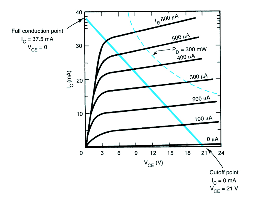
Figure 2. Characteristic Curves for Load Line Analysis of BJT Amplifiers.
The second load-line point is in the saturation region. This point assumes full conduction of $I_{C}$. Ideally, when a transistor is fully conductive:
$$V_{CE}=0 $$
and
$$I_{C}=\frac{V_{CC}}{R_{L}} $$
The two load-line construction points for the analysis circuit are shown on the collector family of characteristic curves of Figure 2. The cutoff point is located at the zero $I_{C}$, 21 V $V_{CE}$ point. The value of $V_{CC}$ determines this point. At cutoff, $V_{CE}$ is equal to $V_{CC}$. The saturation, or full-conduction, point is located at 37.5 mA of $I_{C}$ at 0 V $V_{CE}$. The $I_{C}$ value is calculated using $V_{CC}$ and the value of $R_{L}$. The formula is:
$$I_{C}=\frac{V_{CC}}{R_{L}} $$
Therefore:
$$I_{C}=\frac{21\ \text{V}}{560\ \Omega}=0.0375\ \text{A}=37.5\ \text{mA} $$
These two points are connected by a straight line. The load line makes it possible to determine the operating conditions of the amplifier. For linear amplification, the operating point should be located near the center of the load line. For the circuit in Figure 1, an operating point of 300 $\mu$A of base current is selected. In the circuit diagram, the value of $R_{B}$ determines $I_{B}$. It is calculated by the following equation:
$$I_{B}=\frac{V_{CC}}{R_{B}} $$
The value is:
$$I_{B}=\frac{21\ \text{V}}{70\ \text{k}\Omega}=300\ \mu\text{A} $$
The operating point for this value is located at the intersection of the load line and the 300-$\mu$A $I_{B}$ curve. It is indicated as point Q. Knowing this much about an amplifier shows how it will respond in its static state. The Q point shows how the amplifier will respond without an applied signal.
The collector family of curves in Figure 2 displays the operation of the amplifier in its static state. Projecting a line from the Q point to the $I_{C}$ scale shows the resulting collector current. In this case, the $I_{C}$ is 17.5 mA. The DC beta for the transistor at this point is determined by the following formula:
$$\beta_{dc}=\frac{I_{C}}{I_{B}}$$
This value is:
$$\beta_{dc}=\frac{17.5\ \text{mA}}{30\ \mu\text{A}}=\frac{0.0175\ \text{A}}{0.000030\ \text{A}}=583.3$$
The resulting $V_{CE}$ that will occur for the amplifier can also be determined graphically. Projecting a line directly down from the Q point shows the value of $V_{CE}$. In our circuit, $V_{CE}$ is approximately 11 V. This means that 10 V will appear across $R_{L}$ when the transistor is in its static state.
Dynamic Load Line Analysis
Static load-line analysis focuses solely on DC biasing conditions without any input signal, establishing a single Q point. In contrast, dynamic load-line analysis considers the behavior of the amplifier when an AC signal is applied, showing how the operating point moves along the load line. This approach provides a more complete picture of amplifier operation during actual signal conditions, including effects on output waveform, distortion, and gain.
Dynamic load-line analysis shows how an amplifier responds to an AC signal. In this case, the collector family of curves and the circuit of Figure 3 are used. A load line and Q point for the circuit have been developed on the curves. This establishes the static operation of the amplifier. Note the values of $V_{CE}$ and $I_{C}$ in the static state.
Assume that a 0.1-V peak-to-peak AC signal is applied to the input of the amplifier and the signal causes a 20-$\mu$A peak-to-peak change in $I_{B}$. During the positive alternation of the input shown on the right of Figure 3, $I_{B}$ changes from 30 to 40 $\mu$A. This is shown as point P on the load line. During the negative alternation, $I_{B}$ drops from 30 to 20 $\mu$A. This is indicated as point N on the load line. In effect, this means that 0.1 V peak-to-peak causes $I_{B}$ to change 20 $\mu$A peak-to-peak. The $I_{B}$ signal extends to the right of the load line. Its value is shown as $\Delta I_{B}$ ($\Delta I_{B} = 40 – 20 , \mu A = 20 , \mu A$).
To show how a change in $I_{B}$ influences $I_{C}$, lines are projected to the left side of the load line of Figure 3. Note the projection of lines P, Q, and N toward the $I_{C}$ values. The changing value of $I_{C}$ is indicated as $\Delta I_{C}$. An increase and decrease in $I_{B}$ causes a corresponding increase and decrease in $I_{C}$. This shows that $I_{C}$ and $I_{B}$ are in phase ($\Delta I_{C} = 7.6 – 4.2 , \text{mA} = 3.4 , \text{mA}$).
The AC beta ($\beta_{ac}$) of the amplifier can be determined by $\Delta I_{C}$ and $\Delta I_{B}$. First, determine the peak-to-peak $\Delta I_{C}$ and $\Delta I_{B}$ values. These values are approximations from the characteristic curve load line:
$$\Delta I_{C} = 3.4 , \text{mA}$$
$$\Delta I_{B} = 20 , \mu A$$
Then divide $\Delta I_{C}$ by $\Delta I_{B}$ to determine the AC beta of the amplifier circuit:
$$\beta_{ac} = \frac{\Delta I_{C}}{\Delta I_{B}} = \frac{3.4 , \text{mA}}{20 , \mu A} = \frac{0.0034 , \text{A}}{0.00002 , \text{A}} = 170$$
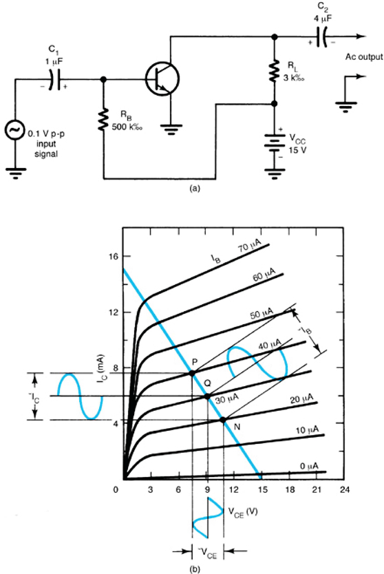
Figure 3. Dynamic load line. (a) Circuit. (b) Characteristic curves.
The same procedure can be used to determine the DC beta of the transistor at point Q:
$$\beta_{dc} = \frac{I_{C}}{I_{B}} = \frac{5 , \text{mA}}{30 , \mu A} = \frac{0.005 , \text{A}}{0.00003 , \text{A}} = 167$$
Note that the AC and DC beta values of this amplifier are similar. These values should be similar within the normal operating range of the transistor.
Projecting points P, Q, and N downward from the load line shows how $V_{CE}$ changes with $I_{B}$. The value of $V_{CE}$ is indicated as $\Delta V_{CE}$. Note that an increase in $I_{B}$ causes a decrease in the value of $V_{CE}$. A decrease in $I_{B}$ causes $V_{CE}$ to increase. This shows that $I_{B}$ and $V_{CE}$ are 180$^{\circ}$ out of phase. The difference in $V_{CE}$ at any point appears across $R_{L}$.
The AC voltage gain of the amplifier can be determined from the dynamic load line. Remember that a 0.1-V peak-to-peak input caused a change of 20-$\mu$A peak-to-peak in the $I_{B}$ signal. The AC voltage gain can be determined by dividing $\Delta V_{CE}$ by $\Delta V_{B}$. The $\Delta V_{B}$ value is 0.1-V peak-to-peak. Using the $\Delta V_{CE}$ value from the graph and $\Delta V_{B}$, determine the AC voltage gain of the amplifier circuit ($\Delta V_{CE} = 11 – 7.5 , \text{V} = 3.5 , \text{V}$):
$$A_{V(ac)} = \frac{\Delta V_{CE}}{\Delta V_{B}} = \frac{3.5 , \text{V}{pp}}{0.1 , \text{V}{pp}} = 35$$
Key Takeaways
Transistor load line analysis serves as a critical tool in understanding both the static and dynamic behaviors of amplifier circuits. By employing graphic methods to develop load lines and characteristic curves, engineers can predict circuit responses and optimize designs for specific applications. The ability to visualize static states—through the establishment of the Q point—and dynamic changes—by considering variations in input signals—enables a comprehensive understanding of performance characteristics such as linearity, gain, and distortion.