This article explains the basic circuitry, static operation, and dynamic behavior of the BJT common emitter amplifier, highlighting how biasing and signal amplification are achieved using bipolar junction transistors.
The primary function of an amplifier is to provide voltage gain, current gain, or power gain. The resulting gain depends a great deal on the device used, its circuit components, and its circuit configuration. Proper component selection and circuit bias are needed to maintain a stable operating point. A stable operating point ensures that the amplifier output will not enter cutoff or saturation due to changes in temperature. In this article, you will learn about the basic circuitry and operation of a common emitter amplifier circuit.
For a bipolar junction transistor (BJT) to respond as an amplifier, the emitter-base junction must be forward-biased, and the collector-base junction must be reverse-biased. Specific operating voltage values must be selected that will permit amplification.
Normally, an amplifier circuit is energized by a DC voltage. An AC signal is then applied to the input of the amplifier. After passing through the transistor, an amplified version of the signal appears in the output. Operating conditions of the transistor and the circuit determine the level of amplification to be achieved.
If both reproduction and amplification are to be achieved, the device must operate in the center of its active region. Remember that this is between the saturation and cutoff regions of the collector family of characteristic curves. Proper circuit component selection permits a transistor to operate in the active region.
Common-Emitter Amplifier Circuit
Look at the circuit diagram of a basic amplifier shown in Figure 1. Note that a schematic symbol of the NPN transistor is used in this diagram. While you study this circuit, keep in mind the crystal structure of the device represented by the symbol.
The basic amplifier has a number of parts that are needed to make it operational. $V_{CC}$ is the DC energy source. The negative side of $V_{CC}$ is connected to ground. The emitter is also connected to ground. This type of circuit configuration is called a grounded-emitter amplifier, or common-emitter amplifier. The emitter, one side of the input, and one side of the output are commonly connected together. In an actual circuit, these points are usually connected to ground.
The base resistor ($R_{B}$) of the basic amplifier is connected to the positive side of $V_{CC}$. This connection makes the base positive with respect to the emitter. The emitter-base junction is forward-biased by $R_{B}$. Resistor $R_{L}$ connects the positive side of $V_{CC}$ to the collector. This connection reverse biases the collector. Through the connection of $R_{B}$ and $R_{L}$, the transistor is properly biased for operation. A transistor connected in this manner is considered to be in its static state, or DC operating state. It has the necessary DC energy applied to be operational. No signal is applied to the input for amplification.
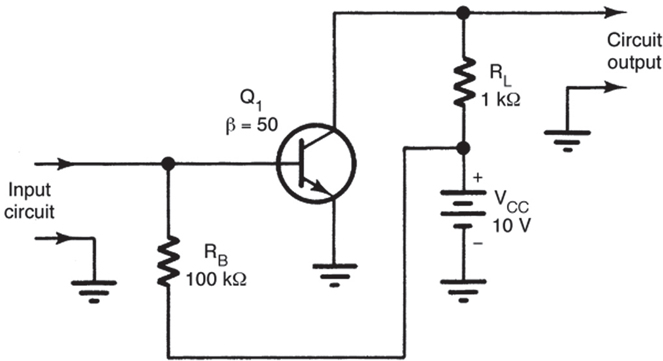
Figure 1. Basic BJT Amplifier Circuit Diagram
Amplifier Operation in Static-State
Let us now consider the operation of the basic amplifier in its static state. With the given values of Figure 2, the base current ($I_{B}$) can be calculated. $I_{B}$, in this case, is limited by the value of $R_{B}$ and the base-emitter junction resistance. When the base-emitter junction is forward-biased, its resistance becomes very small. The value of $R_{B}$ is, therefore, the primary limiting factor of $I_{B}$. $I_{B}$ can be determined by an application of Ohm’s law:
$$I_{B}=\frac{V_{CC}}{R_{B}}$$
For our basic transistor amplifier, this is determined to be
$$I_{B}=\frac{10}{100,000}$$
$$I_{B}=0.0001 \, A \quad \text{or} \quad 100 \, \mu A$$
The value of base current, in this case, is extremely small. Remember that only a small amount of $I_{B}$ is needed to produce $I_{C}$.
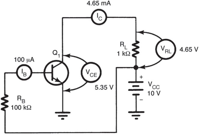
Figure 2. Static Operating Condition of a BJT Amplifier
The beta of the transistor used in Figure 2 has a given value. With beta and the calculated value of $I_{B}$, it is possible to determine the collector current of the circuit. Beta is the current gain of a common-emitter amplifier. Beta is described by the following formula:
$$\beta=\frac{I_{C}}{I_{B}}$$
In our transistor amplifier, $I_{B}$ has been determined, and beta has a given value of 50. By transposing the beta formula, $I_{C}$ can be determined by the following equation:
$$I_{C}=\beta\times I_{B}$$
For the amplifier circuit, the collector current is determined to be
$$I_{C}=50\times 100\mu A$$
$$I_{C}=50\times 0.0001\,A$$
$$I_{C}=0.005\,A\quad\text{or}\quad 5mA$$
This means that 5 mA of $I_{C}$ will flow through $R_{L}$ when an $I_{B}$ of 100 $\mu$A flows.
In any electric circuit, we know that current flow through a resistor causes a corresponding voltage drop. In a basic transistor amplifier, $I_{C}$ causes a voltage drop across $R_{L}$. Take a look at Figure 2. In the preceding step, $I_{C}$ was calculated to be 5 mA. By using Ohm’s law again, we can determine the voltage drop across $R_{L}$ from the following equation:
$$V_{RL}=I_{C}\times R_{L}$$
For the amplifier circuit, the voltage drop across $R_{L}$ is:
$$V_{RL}=5\,mA\times 1k\Omega$$
$$V_{RL}=0.005\,A\times 1000\Omega$$
$$V_{RL}=5V$$
This means that half or 5 V of $V_{CC}$ will appear across $R_{L}$. With a $V_{CC}$ value of 10 V, the other 5 V will appear across the collector-emitter of the transistor. This is determined by:
$$V_{CE}=V_{CC}-V_{RL}$$
Thus,
$$V_{CE}=10V-5V$$
$$V_{CE}=5V$$
A $V_{CE}$ voltage of 5 V from a $V_{CC}$ of 10 V means that the transistor is operating near the center of its active region. Ideally, the transistor should respond as a linear amplifier.
The operational voltage and current values of the basic transistor amplifier in its static state are summarized in Figure 2. Note that an $I_{B}$ of 100 $\mu$A causes an $I_{C}$ of 5 mA. With a beta of 50, the amplifier has the capability of a substantial amount of output current. The collector current passing through $R_{L}$ causes VCC to be divided. This establishes operation in the approximate center of the collector family of characteristic curves. Ideally, this static condition should cause the amplifier to respond as a linear device when a signal is applied.
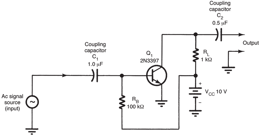
Figure 3. Amplifier with an AC signal applied.
Example 1
From the values provided in Figure 2, determine base current ($I_{B}$), collector current ($I_{C}$), load resistor voltage ($V_{RL}$), and collector-emitter voltage ($V_{CE}$).
Solution:
Determine the base current:
$$I_{B}=\frac{V_{CC}}{R_{B}}=\frac{12}{200,000}=60\mu A$$
Using the given beta ($\beta$) and calculated base current:
$$I_{C}=\beta\times I_{B}=100\times 60\,\mu A=6\,mA$$
Determine the voltage across the load resistor:
$$V_{RL}=I_{C}\times R_{L}=6\,mA\times 1000\,\Omega=6\,V$$
Determine the collector-emitter voltage:
$$V_{CE}=V_{CC}-V_{RL}=12\,V-6\,V=6\,V$$
Signal Amplification
For the basic transistor circuit of Figure 2 to respond as an amplifier, it must have a signal applied. This signal is made up of voltage and current components. The applied signal causes the transistor to change from a static condition to a dynamic condition. Dynamic conditions involve changing values. All AC amplifiers respond in the dynamic state.
Figure 3 shows a basic transistor amplifier with an AC signal applied. A capacitor is used in this case to couple the AC signal source to the amplifier. AC passes easily through a capacitor, whereas DC is blocked. As a result, the AC signal is injected into the base-emitter junction. DC does not flow back into the signal source. The AC signal is, therefore, added to the DC operating voltage. The emitter−base voltage is a DC value that changes at an AC rate.
Consider how the applied AC signal alters the emitter-base junction voltage. Figure 5 shows some representative voltage and current values that appear at the emitter−base junction of the transistor.
They can be measured with a voltmeter or observed with an oscilloscope. Figure 5(a) shows the DC operating voltage and base current. This occurs when the amplifier is in its steady or static state. Figure 5(b) shows the AC signal that is applied to the emitter−base junction. Note that the amplitude change of this signal is a very small value. This also shows how the resulting voltage and base current change with an AC signal applied. The AC signal essentially rides on the DC voltage and current.
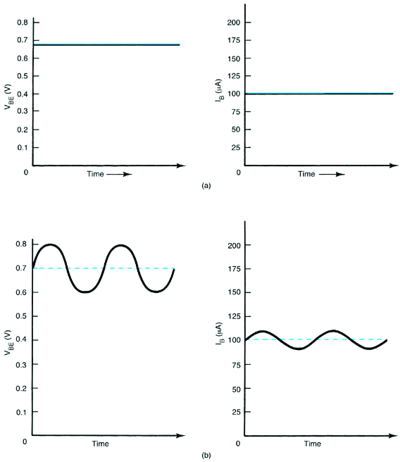
Figure 5. $I_{B}$ and $V_{BE}$ Conditions (a) Static, (b) Dynamic
Refer to the schematic diagram of the basic amplifier in Figure 6. Note the waveform inserts that show the current and voltage responses when an AC signal is applied. They also show where instruments are connected to measure and observe these values.
The AC signal applied to the input rises during the positive alternation and falls during the negative alternation. Initially, this causes an increase and a decrease in the value of $V_{BE}$. This voltage has a DC level with an AC signal riding on it. The indicated $I_{B}$ is developed as a result of this voltage.
The changing value of $I_{B}$ causes a corresponding change in $I_{C}$. $I_{B}$ and $I_{C}$ appear similar in waveforms but differ vastly in magnitude. $I_{B}$ is in microamperes; $I_{C}$ is in milliamperes.
The resulting $I_{C}$ passing through $R_{L}$ causes a corresponding voltage drop across $R_{L}$. $V_{CE}$ across the transistor is the reverse of $V_{RL}$. These signals are both AC values riding on a DC level. The output, $V_{out}$, is changed to a pure AC value. Capacitor $C_{2}$ blocks the DC component and passes only the AC signal.
It is interesting to note that in Figure 6, the input and output signals of the amplifier are reversed. When the positive alternation of the AC input signal rises in value, it causes the output to fall in value. The negative alternation of the input causes the output to rise in value. This condition of operation is called phase inversion. It is shown by the output or VCE waveform appearing across the emitter−collector. Phase inversion is a distinguishing characteristic of the common-emitter amplifier.
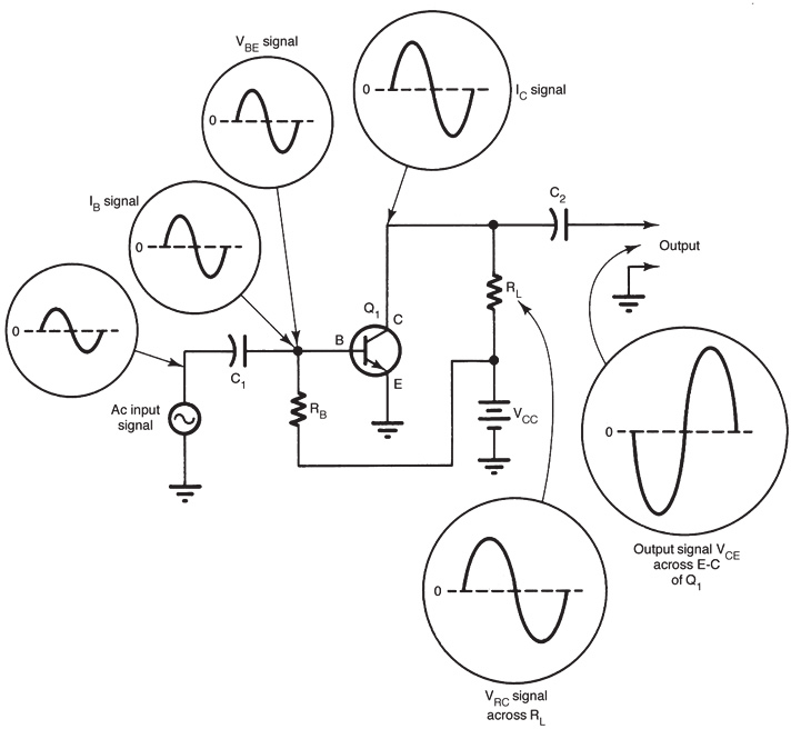
Figure 6. BJT Amplifier Operation
Review Questions
- In a BJT amplifier, the _______ junction must be forward biased, and the _______ junction must be reverse biased.
- The primary function of an amplifier is to provide _______, _______, or _______ gain.
- The base resistor is labeled as _______ in the amplifier circuit.
- The equation to find base current is _______.
- Phase inversion is a characteristic of a _______ amplifier.
Answers
- emitter-base, collector-base
- voltage, current, power
- $R_{B}$
- $I_{B}=\frac{V_{CC}}{R_{B}}$
- common-emitter
Common Emitter Amplifier Key Takeaways
BJT amplifiers rely on proper biasing to maintain operation within the active region, ensuring stable signal amplification. A small base current effectively controls a much larger collector current, enabling significant amplification with minimal input. Understanding the static conditions establishes the amplifier’s baseline performance, while the dynamic conditions reveal how the circuit responds to applied AC signals. Additionally, phase inversion, a distinct feature of the common-emitter configuration, plays a critical role in shaping the output waveform relative to the input.