The article covers the fundamental behavior of transistor through characteristic curves, focusing on how collector current varies with base current and collector-emitter voltage. It also explains the transistor’s operating regions—cutoff, saturation, and active—and introduces the concept of the load line and operating point for analyzing transistor behavior in circuits.
A fundamental property of a transistor and how it works is pointed out in the following Figure, where a transistor is correctly biased by two power supplies.
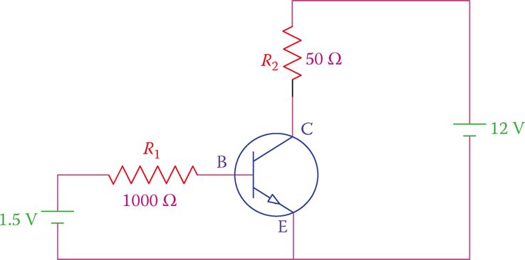
Figure: Transistor Working with Two Power Supplies
Figure 1 shows a simple circuit of a transistor, in which the 1.5 V battery and the resistance RB determine the base current IB, and the 24 V battery together with RC define the collector current IC. We are interested in determining the variation of the collector current IC. This current can be varied either by changing the base current IB or the collector-emitter voltage VCE (the voltage between the collector C and the emitter E). The base current can be varied by the variable resistor RB.
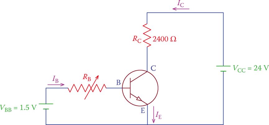
Figure 1 Simple circuit for a transistor operation.
The characteristic curves of a transistor provide the relationship between collector-emitter voltage and collector current for different values of the base current. Because there are two parameters that affect IC, a set of individual curves shown together denote various operating conditions.
A typical curve is shown in Figure 2a, and a set of these curves are depicted in Figure 2b. Each individual curve depicts the variation of IC versus the value of collector-emitter voltage (VCE) for a fixed value of base current IB.
When IB is zero, a transistor is cut off, and it does not conduct no matter how much voltage is applied to the collector; any collector current is due to leaks, is very small, and is negligible. In both Figure 2a and b, the curve corresponding to IB = 0 is exaggerated for clarity.
The area under the curve corresponding to IB = 0, shaded in Figure 2a, represents the region where a transistor is cut off and is not conducting.
Saturation Region
For each nonzero value of IB, the collector current starts from zero when the collector-emitter voltage is zero. A transistor starts conducting and the collector current increases rapidly when VCE > 0. The area around this abrupt change in IC also shaded in Figure 2a, corresponds to when a transistor is in saturation.
Saturation implies that the collector current has reached its maximum value for that collector-emitter voltage and cannot increase further by increasing the base current IB. For example, consider point M corresponding to VCE = VM in Figure 2b. For this point, IC has reached its maximum and cannot be increased by increasing IB. In contrast, an increase in IB can move point N to N′, both corresponding to a collector-emitter voltage VN.
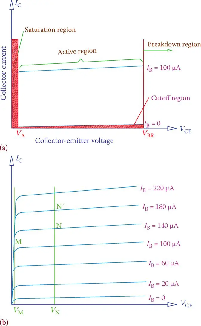
Figure 2 Collector current versus collector voltage characteristic curve of a transistor. (a) For one value of base current. (b) For multiple values of base current.
Saturation (in a transistor): The state of a transistor at which the collector current has reached its maximum value for the present collector-emitter voltage, and cannot increase further by only increasing the base current IB.
The meaning of transistor saturation is better demonstrated in Figure 3, in which the scale of the horizontal axis is augmented so that the line segments with sharp slopes can be better displayed.
Two characteristic curves, corresponding to two base currents IB1 and IB2 are shown. Suppose that the collector-emitter voltage is 2 V. On both curves the corresponding point is A. This implies that if the base current is increased to IB2, but the VCE is still 2 V, the collector current does not change. The collector current increases only if the VCE increases, for instance, to 4 V, for which the operating point moves from A to B.
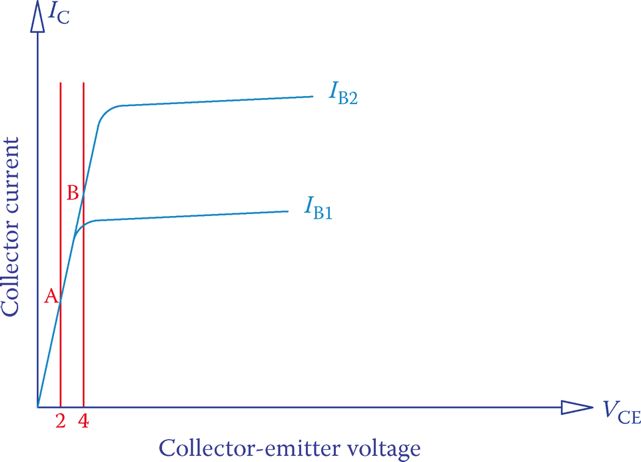
Figure 3 Typical set of characteristic curves for a transistor.
Active Region
When saturated, a transistor cannot operate as expected. In normal operation, transistors function in the active region, the area that the characteristic curve is a segment of an almost horizontal straight line. In this region increasing collector-emitter voltage has little effect on the collector current. In other words, the transistor exhibits a large resistance in this region, so that increasing voltage has little effect on the current through it. This resistance is variable because it depends on the value of IB (for each value of IB the ratio VCE/IC is different).
Active region: An area in the characteristic curve of a transistor, in terms of collector-emitter voltage and collector current values that the transistor can function. If any of these values falls outside of its range a transistor falls in the saturation region or cutoff region and cannot function (see Figure 2a).
The active region is between the two voltages denoted by VA and VBR in Figure 2a. If VCE surpasses the breakdown voltage VBR, the transistor gets damaged, and if VCE < VA, the transistor is in a saturation state.
Breakdown voltage: Voltage at which a semiconductor device changes behavior or gets damaged.
The operating point of a transistor is a point on these curves, corresponding to a given IB and a given value for VCE. A transistor, nevertheless, cannot work at all the possible points that can be found on the characteristic curves. This is because of the physical limitations of a transistor in handling a collector current without getting overheated and damaged. The limiting power boundary is shown in Figure 4 by the dashed curve for a typical transistor.
It is possible to run the transistor in all the points to the left of the dashed curve, but not on the region on the right side of this curve. In this region, either IC is high or VCE is high, resulting in relative high-power consumption in a transistor, which converts to heat.
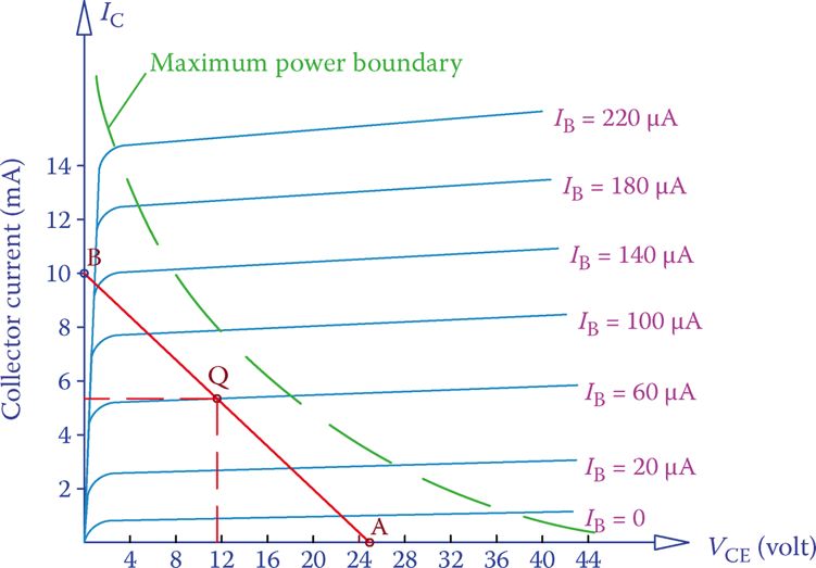
Figure 4 Operating point and boundary curve for the maximum power capacity of a transistor.
The operating point for a transistor (represented by Q in Figure 4), under the operating conditions governed by the supply voltage VCC and the base voltage VBB (see Figure 1) and the resistances RB and RC, is at the intersection of lines corresponding to VCE and the base current.
For a constant set of values for VCC, VBB, and RC if RB is varied the value of IB, and consequently IC and VCE, change. Each pair of IC and VCE defines an operating point denoted by Q. When as a result of varying RB, while the parameters VCC, VBB, and RC are kept constant, the values of the collector-emitter voltage VCE and collector current IC vary, this point Q moves on a straight line AB, as shown in Figure 4.
VCE is obtained from the supply voltage VCC minus the voltage drop in RC (and any other resistor in the collector-emitter loop connected to VCC).
In the cutoff state, the current through RC is zero and no voltage is dropped in RC (and any other resistor in series with RC in the same loop). Consequently, all the applied voltage (VCC) appears at the collector. This defines point A of the line, where VCE is maximum.
Also, if a transistor is conducting, but there is no internal resistance between C and E, this defines the maximum current that the collector can have (point B of the line). This maximum current can be found by dividing VCC by all the resistors in the loop (only RC in Figure 1). Thus, for a given supply voltage VCC, the collector current can vary between zero (at point A) and a maximum value (at point B), as the line AB shows.
The intersection of the line AB with one of the transistor characteristic curves defines the operating point Q. The line AB is called the load line. The load line, thus, represents all the possible locations of point Q for a transistor in a given circuit with constant VCC and resistance(s) in the collector-emitter circuit.
Load line (in a transistor): Line showing the operating points of a transistor on a transistor characteristic curve, based on the supply voltage and the resistors in the transistor circuit. This line is between the points corresponding to the maximum collector voltage and maximum collector current.
Transistor Characteristic Curves Example 1
For the transistor shown in Figure 1, whose characteristic curves are shown in Figure 4, if the base current is 60 μA, find the collector current and the value of ß.
Solution
The maximum current through the collector is defined by dividing the supply voltage (24 V) by the resistor RC. Thus, point B end of the load line on the current (vertical) axis is at
\[\frac{24}{2400}=10mA\]
The other end of the load line (point A) is on the horizontal axis at 24 V. This line is the same as shown in Figure 4 and intersects the curve corresponding to 60 μA base current at point Q (as shown).
Dropping a perpendicular from Q to the vertical axis gives the current in the collector. On the basis of the figure, this current is 5.5 mA.
The value for ß can be found from dividing collector current by the base current.
\[\frac{5.5mA}{60\mu A}=\frac{5500\mu A}{60\mu A}\approx 92\]
Example 2
If in Example 1 the supply voltage changes to 30 V and RC is 2200 Ω (other parameters remaining unchanged), how much are IC and VCE?
Solution
A new load line needs to be drawn on the same graph of Figure 4. The intersection of this line with the line corresponding to IB = 60 μA defines the values of IC and VCE.
Point A for this new line is at VCE = 30 V, thus between 28 and 32 (not shown), and point B is at IB = 30 ÷ 2200 = > 13.6 mA. If you draw this line you will find its intersection with 60 μA base current, which corresponds to IC = 5.6 mA and VCE = 17.4 V.
Transistor Characteristic Curves Key Takeaways
Understanding the characteristic curves, operating regions, load line, and operating point of a transistor is essential for designing and analyzing electronic circuits. These concepts are crucial because they determine how a transistor behaves under different conditions, allowing engineers to use transistors effectively as amplifiers or switches in real-world applications. Whether in audio amplifiers, signal processing, or digital logic circuits, accurate control over the transistor’s operating point ensures reliable performance and prevents damage from overcurrent or overheating.