This article introduces power electronic interfaces used in microgrids, explaining their role in integrating distributed energy resources and managing voltage, frequency, and power conversion. It provides an overview of DC–DC converters and DC–AC inverters, describing common topologies and control concepts that enable efficient and flexible power processing.
Power electronic interfaces improve the quality and value of electricity, from generation to utilization. Commonly, power electronic interfaces are used when integrating distributed energy resources to microgrids. The power electronic interface does not store electrical energy but converts the power received from the distributed energy resources to a desired voltage and frequency. Some of the important functions of power electronic interfaces can be presented as follows.
Integration requirements: When multiple distributed energy resources are available in a microgrid, the different characteristics of the components mean that power conversion (AC to DC, DC to AC, DC to DC, AC to AC) is required. Depending on the architecture of the microgrid, as AC, DC, or hybrid, the power electronic interface units required may vary. In addition to that, power electronic interfaces play an important role in maintaining the interaction with the main grid.
Operational requirements: When solar PV generation is available, maximum power point tracking (MPPT) is required to enhance the efficiency. MPPT is an important concept related to solar PV systems, such that solar PV systems operate by extracting the maximum possible power at every instance. Most of the advanced power electronic interface units for solar PV systems have the MPPT feature.
DC to DC Converters
A DC-to-DC converter is a power electronic interface that converts the voltage level of a DC source to another level. There are two main types of DC-to-DC converters, linear and switched, based on the method of conversion.
Linear DC to DC converters: As the name implies, a linear converter regulates the output DC voltage using a linear component. For example, a resistive load can be used in a linear DC to DC converter such that a resistive voltage drop regulates the output voltage level. The general structure of a linear DC to DC converter is given in Figure 1.
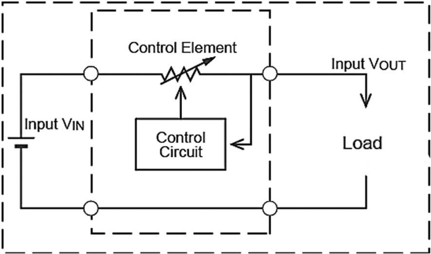
Figure 1. Linear DC to DC Converter Circuit Diagram
Switched DC to DC converters: In switched mode converters, the input energy is stored in a periodic manner and released to obtain an output voltage at a desirable level. Inductors, transformers, and capacitors can be used as energy-storing components. The general structure of a switched DC to DC converter is given in Figure 2.
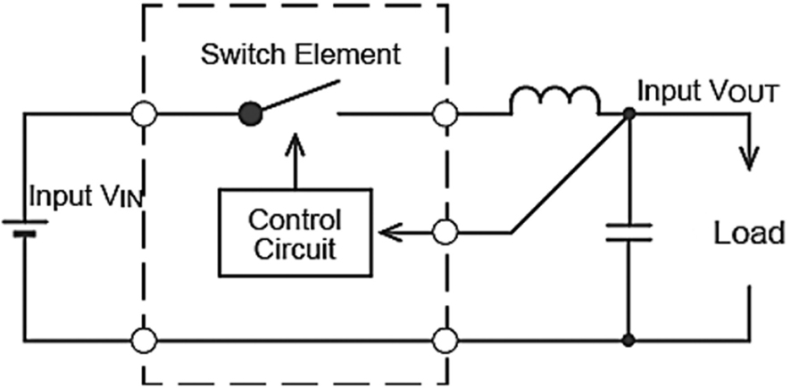
Figure 2. Switched DC to DC Converter Circuit Diagram
To be specific, the input power supply is converted to a voltage pulse by the switching element in the circuit. The capacitors, inductors, and other elements smooth the generated voltage pulse. The power is supplied from the input side to the output by turning ON a switch (such as a MOSFET: a Metal–Oxide–Semiconductor Field-Effect Transistor, which is a field-effect transistor where the voltage determines the conductivity of the device, and which is used for switching or amplifying signals) until the desired voltage is reached. Once the output voltage reaches the predetermined value, the switch element is turned OFF, and no input power is consumed. This operation is repeated at high speeds to improve the efficiency of the converter and to reduce thermal losses.
A comparison between linear and switched DC to DC converters is presented in Table 1.
Table 1. Comparison between Linear and Switched Converters
| Linear Converters | Switched Converters |
| Simpler configuration | Complicated configuration |
| Requirement for a few external components | Requirement for more external components |
| Lower noise | Higher noise |
| Only DC/DC step-down (buck) operation | Supports buck, boost, buck–boost, etc. operations |
| Comparatively lower efficiency | Comparatively higher efficiency |
| Significant heat generation | High-frequency switching operation lowers the heat generation |
Switched DC to DC converters can be categorized based on the electrical isolation of the circuit, as shown in Figure 3. The term “isolation” refers to whether or not the input and the output of the DC-to-DC converter are electrically separated. In an isolated DC to DC converter, a transformer is included in the circuit such that the DC path between the input and the output is eliminated. Unlike an isolated converter, a non-isolated DC to DC converter consists of a DC path between the input and the output.
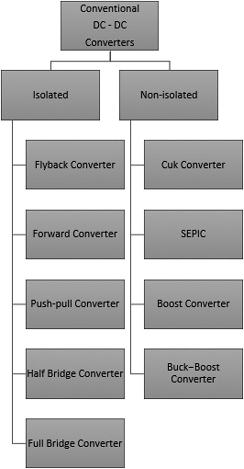
Figure 3. Categorization of conventional DC to DC converters
Let’s analyze the characteristics and operation of buck, boost, and buck–boost converters. In DC to DC converters, the operation of semiconductor switches such as insulated gate bipolar transistors (IGBTs) or MOSFETs occurs periodically. Let’s take the operational period as Ts. The switch is closed and opened for times TON and TOFF, respectively. The duty ratio D of the converter is the ratio between the active time of the converter and the switching period, as given in equation (1).
$$ D=\frac{T_{ON}}{T_{s}} =\frac{T_{ON}}{T_{ON+T_{OFF}}} (1) $$
Buck Converter
A buck converter reduces the input DC voltage to a specified DC output voltage. A typical buck converter is shown in Figure 4.
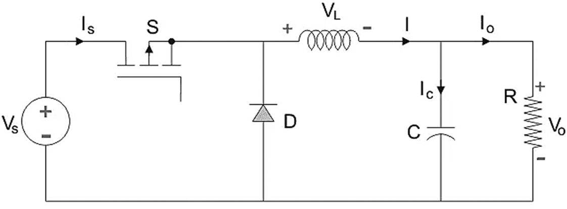
Figure 4. Buck DC/DC converter topology
The input voltage source is coupled to a switch-like controlled solid-state device. A Power MOSFET or an IGBT can be used as the solid-state device. Thyristors are not commonly used in DC-to-DC converters because turning off a thyristor in a DC-to-DC circuit necessitates another commutation, which necessitates the use of another thyristor, whereas Power MOSFETs and IGBTs can be turned off by simply setting the voltage between the GATE and SOURCE terminals of the Power MOSFET, or the GATE and COLLECTOR terminals of the IGBT, to zero.
A diode is utilized as the second switch. A low-pass LC filter (LC filters are circuits consisting of a combination of inductors (L) and capacitors (C) to cut or pass specific frequency bands of an electric signal) is used to connect the switch and the diode, and is designed to reduce current and voltage ripples. The load is completely resistive. The input voltage is constant, as is the current flowing through the load. The current source can be considered as the load.
Pulse width modulation (PWM) is used to turn on and off the controlled switch. PWM can be based on time or frequency. The use of a wide range of frequencies to accomplish the desired control of the switch, which in turn gives the desired output voltage, is a disadvantage of frequency-based modulation. This necessitates a sophisticated design for the low-pass LC filter, which must handle a wide frequency range.
DC to DC converters commonly use time-based modulation. This is easy to put together and use. In this sort of PWM modulation, the frequency remains constant.
The operation of a buck converter can be discussed for two operating modes as follows.
Mode 1: Switch–ON State, Diode–OFF State
The circuit configuration of a buck converter that operates in Mode 1 is shown in Figure 5. Let’s derive a mathematical model for the buck converter operation in this mode of operation. Here, the voltage across the capacitance can be considered to be equal to the output voltage under the steady state condition.
Here we can consider that the switch is on for a time TON and is off for a time TOFF. We define the time period, T, as in equation (2)
$$ T={T_{ON+T_{OFF}}} (2)$$
and the switching frequency is given in equation (3),
$$ f_{switching}=\frac{1}{T} (3)$$
The duty cycle D was previously defined by equation (1),
$$ D=\frac{T_{ON}}{T_{s}} =\frac{T_{ON}}{T_{ON+T_{OFF}}} $$
For the buck converter operation in steady state for this mode, using Kirchhoff’s Voltage Law,
$$V_{in}=V_{L}+V_{o} (4)$$
$$V_{L}=L\frac{di_{L}}{dt}=V_{in}-V_{o} (5)$$
$$\frac{di_{L}}{dt}=\frac{\Delta i_{L}}{\Delta t}=\frac{\Delta i_{L}}{DT}=\frac{V_{in}-V_{o}}{L} (6)$$
Considering the switch close time TON=DT, we can say that Δt = DT.
$$\left ( \Delta i_{L} \right )_{closed}=\left ( \frac{V_{in}-V_{o}}{L} \right )DT (7)$$
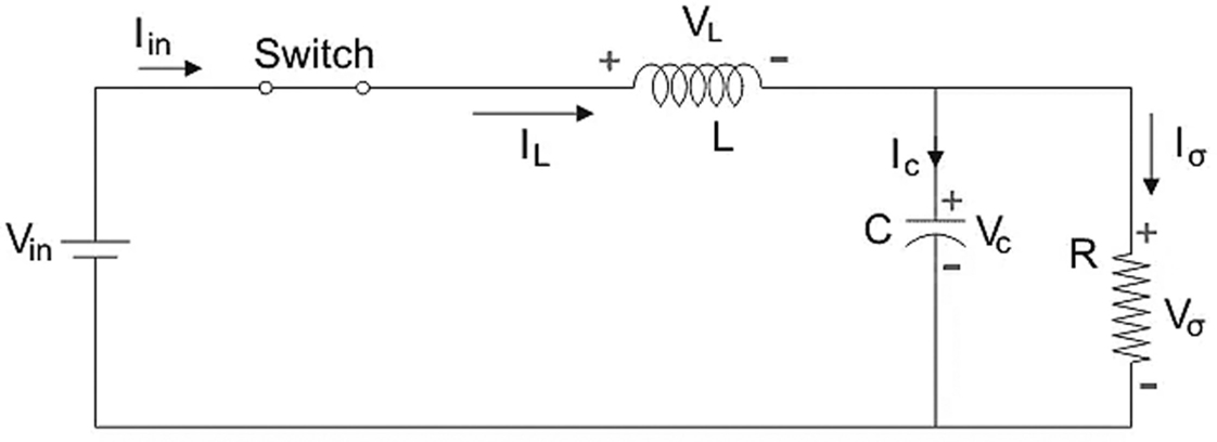
Figure 5. Switch–on state, diode–off state
Mode 2: Switch–OFF State, Diode–ON State
Here, the energy stored in the inductor is released and dissipated in the load resistance, which aids in maintaining current flow through the load. However, when analyzing the circuit with Kirchoff’s Voltage Law, we stick to the original conventions.
The circuit configuration of a buck converter that operates in Mode 2 is shown in Figure 6. For the buck converter operation in steady state for this mode, using Kirchhoff’s Voltage Law,
$$0=V_{L}+V_{o} (8)$$
$$V_{L}=L\frac{di_{L}}{dt}=-V_{o} (9)$$
$$\frac{di_{L}}{dt}=\frac{\Delta i_{L}}{\Delta t}=\frac{\Delta i_{L}}{(1-D)T}=\frac{-V_{o}}{L} (10)$$
Considering the switch open time,
$$T_{OFF}=T-T_{ON}=T-DT=(1-D)T (11)$$
$$\textrm{Taking}\Delta t=(1-D)T$$
$$\left ( \Delta i_{L} \right )_{open}=\left ( \frac{-V_{o}}{L} \right )(1-D)T (12)$$
The net change of the inductor current throughout any complete cycle is already known to be zero.
$$\left ( \Delta i_{L} \right )_{close}+\left ( \Delta i_{L} \right )_{open} =0 (13)$$
$$\left ( \frac{V_{in}-V_{o}}{L} \right )DT+\left ( \frac{-V_{o}}{L} \right )(1-D)T=0 (14)$$
$$\frac{V_{o}}{V_{in}}=D$$
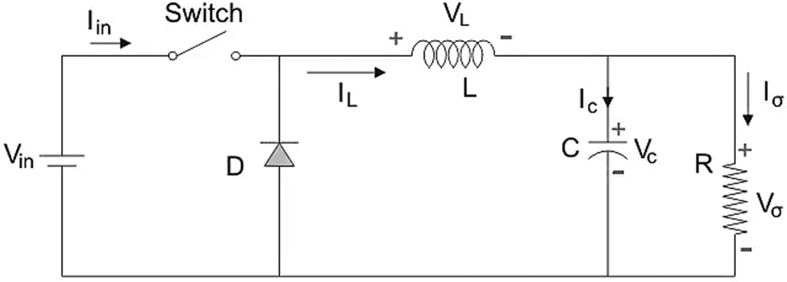
Figure 6. Switch–off state, diode–on state
Boost Converter
A boost converter converts a specific DC input voltage to a DC output voltage. Figure 7 shows an example of a standard boost converter.
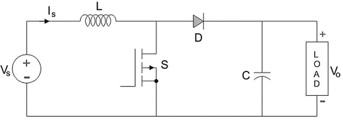
Figure 7. Boost DC/DC converter topology
A mathematical model can be derived for the boost converter in a similar way to the previously discussed buck converter, such that the output voltage is given as,
$$\frac{V_{o}}{V_{in}}=\frac{1}{1-D}$$
Buck–Boost Converter
A buck–boost converter has an output voltage magnitude that is either greater than or less than the input voltage magnitude.
The circuit configuration of a buck–boost converter is shown in Figure 8. A mathematical model can be derived for the buck–boost converter in a similar way to the previously discussed buck converter, such that the output voltage is given as,
$$\frac{V_{o}}{V_{in}}=\frac{D}{1-D}$$
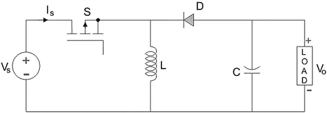
Figure 8. Buck–boost DC/DC converter topology
DC to AC Inverters
Voltage Source Inverter
A VSI is composed of a DC voltage source, a three-phase bridge circuit, and a capacitor with a significantly greater capacitance, as shown in Figure 9.
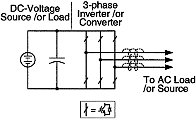
Figure 9. Voltage Source Inverter Circuit Diagram
As listed below, there are two varieties of VSI available.
Square-Wave Inverter Using Gate Turn-Off Thyristor
The DC capacitor input voltage determines the AC output voltage of this converter; hence, the AC output voltage can be varied by adjusting the DC input voltage. The proportionality between the input voltage and the basic component of the output voltage is the main principle of a VSI.
PWM Inverter Using Insulated Gate Bipolar Transistor
Unlike the previous VSI, this one has a constant DC input voltage. The output is modified using the PWM approach, in which the modulator’s modulation index is changed according to the required AC output voltage.
Current Source Inverter
As shown in Figure 10, a CSI consists of a DC source, a three-phase bridge, and a DC source that feeds the main converter circuit. A somewhat large DC inductor fed by a voltage source can be used as the DC source.
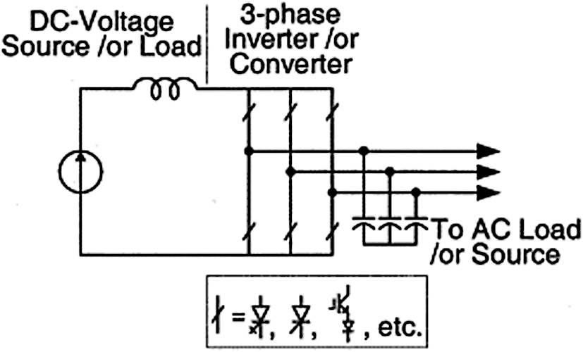
Figure 10. Current Source Inverter Circuit Diagram
Z Source Inverter
A ZSI is composed of a DC source, a two-port network made up of a split-inductor (two inductors, L1, L2), and two capacitors (C1, C2) coupled in an X shape as in Figure 11, and it feeds the main converter circuit with DC via impedance source coupling. A voltage or current source might be used as the DC source. A ZSI provides a simplified single-stage power conversion topology as an added benefit. The shoot-through (ST) can no longer kill the inverter, and it adds DC to DC power conversion (buck–boost mode) to the inverter in addition to DC to AC power conversion. It solves the majority of the issues of traditional voltage and current source inverters.
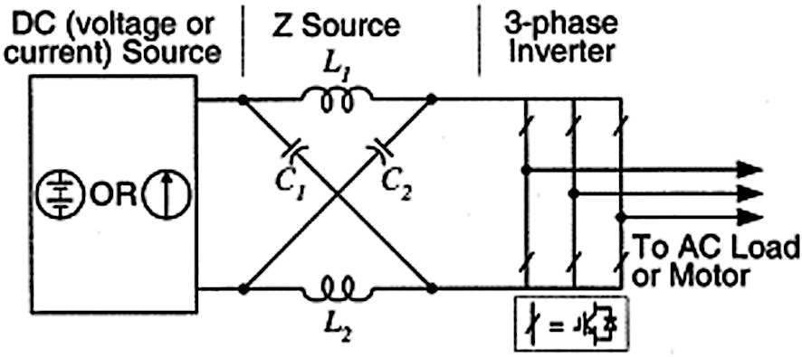
Figure 11. Z source inverter Circuit Diagram
Key Takeaways
Power electronic interfaces are fundamental to modern microgrids because they enable efficient integration, control, and utilization of diverse energy sources with differing electrical characteristics. By supporting flexible voltage conversion, power flow regulation, and advanced control functions, these interfaces allow renewable generation, energy storage, and loads to operate reliably in both grid-connected and islanded modes. Understanding converter and inverter topologies is therefore essential for designing scalable, efficient, and resilient microgrid applications ranging from residential and commercial systems to industrial and community-scale power networks.