The article discusses Insulated-Gate Bipolar Transistors (IGBTs), outlining their construction, control mechanisms, advantages, and providing an application example. IGBTs combine the fast-switching speed of MOSFETs with the low conduction losses of BJTs, making them ideal for various high-power switching applications. The article also highlights their benefits over traditional MOSFETs and BJTs, emphasizing their suitability for high-voltage and high-frequency applications.
IGBT Construction
Power MOSFETs and BJTs can both be used in high-power switching applications. The MOSFET has the advantage of greater switching speed, and the BJT has lower conduction losses. By combining the low conduction loss of a BJT with the switching speed of a power MOSFET, we can begin to approach an ideal switch.
This hybrid device exists and is called an insulated-gate bipolar transistor (IGBT). The IGBT has essentially evolved from power MOSFET technology. Its structure and operation closely resemble a power MOSFET. Figure 1 shows the basic structure of an n-channel IGBT. Its structure resembles an n-channel power MOSFET constructed on a p-type substrate. As shown, it has a gate, emitter, and collector leads.
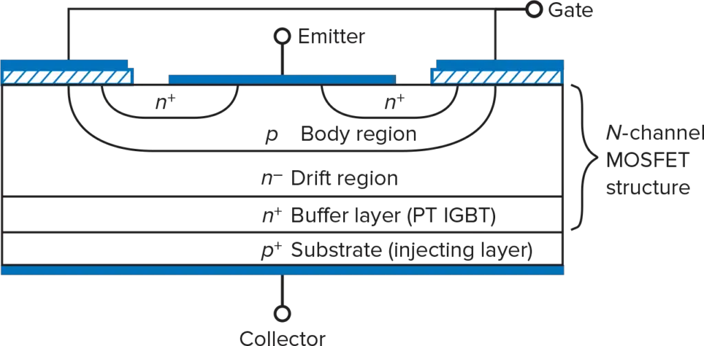
Figure 1. Basic IGBT structure.
Two versions of this device are referred to as punch-through (PT) and nonpunch-through (NPT) IGBTs. Figure 1 shows the structure of a PT IGBT. The PT IGBT has an n+ buffer layer between its p+ and n− regions, and the NPT device has no n+ buffer layer.
NPT versions have higher conduction VCE (on) values than PT versions and a positive temperature coefficient. The positive temperature coefficient makes the NPT suited for paralleling. PT versions, with the extra n+ layer, have the advantage of higher switching speeds. They also have a negative temperature coefficient. Along with the basic structure shown in Figure 1, other IGBTs are manufactured with various advanced technology structures. One such version is the field-stop IGBT (FS IGBT). The FS IGBT combines the advantages of PT and NTP IGBTs while overcoming the disadvantages of each structure.
IGBT Control
Figures 2a and b show two common schematic symbols for an n-channel IGBT. Notice in Figure 2b the intrinsic body-diode. This built-in diode is similar to the body-diodes found in power FETs. Also, figure 2c shows a simplified equivalent circuit for this device. As you can see, the IGBT is essentially a power MOSFET on the input side and a BJT on the output side. The input control is the voltage between the gate and emitter leads. Just as in a power FET, the gate drive circuits for an IGBT must be able to quickly charge up and discharge the IGBT’s input capacitance for fast switching speeds. The output is a current between the collector and emitter leads. Because the output of the IGBT relies on BJT construction, this results in a slower device turn-off speed than a power FET.
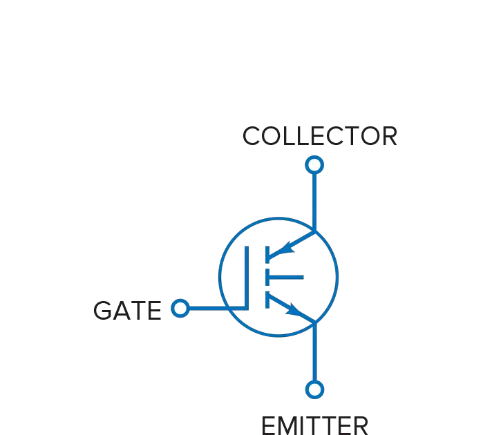
(a) |
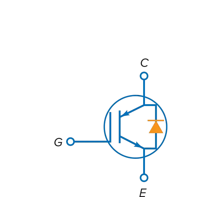
(b) |
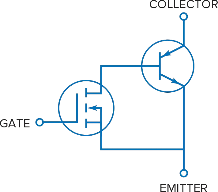
(c) |
Figure 2. IGBTs: (a) and (b) Schematic symbols; (c) simplified equivalent circuit.
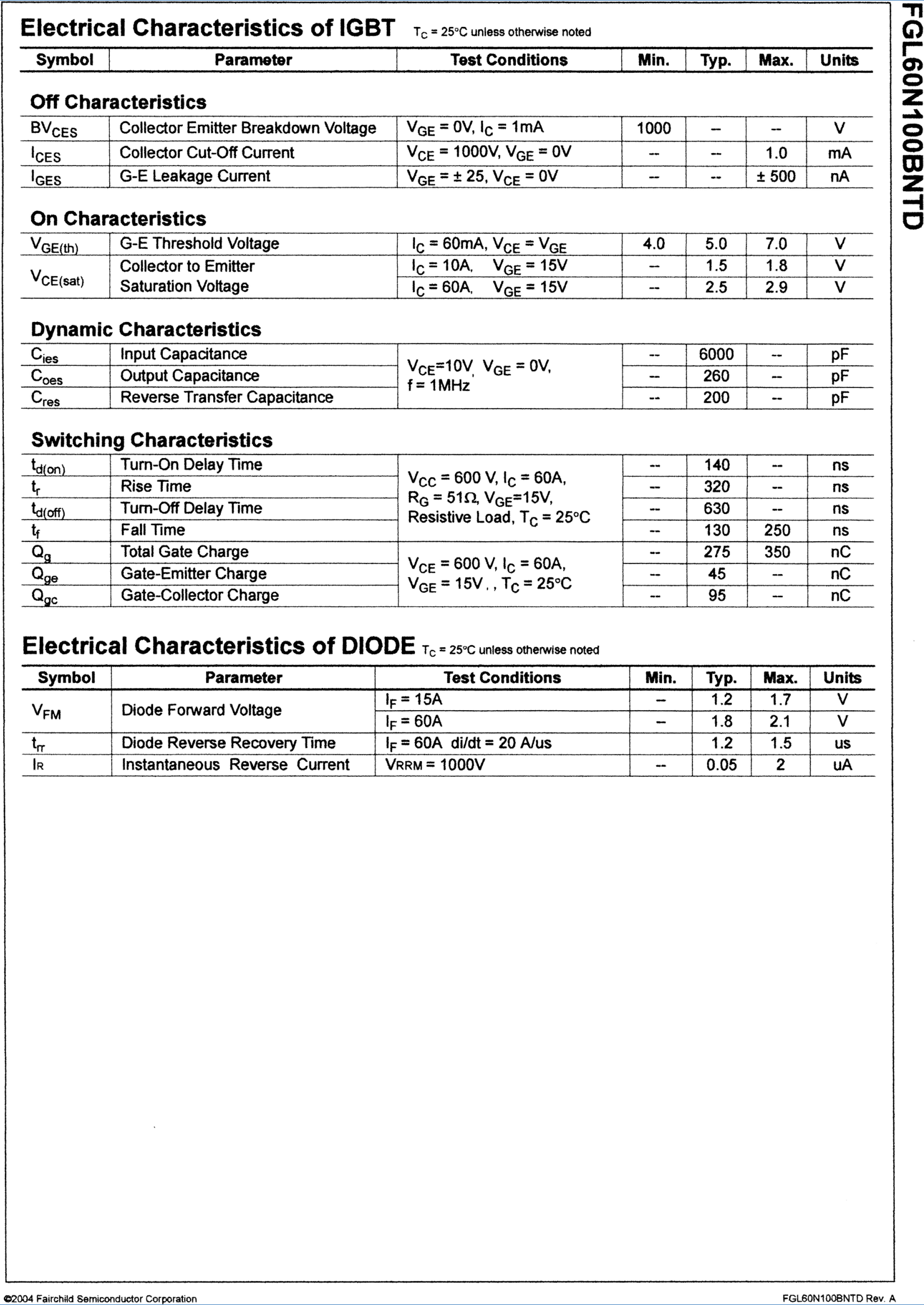
The IGBT is a normally-off high-input impedance device. When the input voltage VGE is large enough, the collector current will begin to flow. This minimum voltage value is the gate threshold voltage VGe(th). Figure 3 shows the data sheet for an FGL60N100BNTD IGBT using NPT-trench technology. The typical VGe(th) for this device is listed as 5.0 V when IC = 60 mA. The maximum continuous collector current is shown to be 60 A. Another important characteristic is its collector-to-emitter saturation voltage VCE (sat). The typical VCE (sat) value, shown on the datasheet, is 1.5 V at a collector current of 10 A and 2.5 V at a collector current of 60 A.

Figure 3. IGBT datasheet with Electrical characteristics
IGBT Advantages
Good To Know
For high-voltage and high- frequency switching power applications, silicon carbide or SiC MOSFETs have advantages over traditional silicon MOSFETs and IGBTs.
Conduction losses of IGBTs are related to the forward voltage drop of the device, and the MOSFET conduction loss is based on its RDS (on) values. For low-voltage applications, power MOSFETs can have extremely low RD (on) resistances. In high-voltage applications, however, MOSFETs have increased RDS (on) values, resulting in increased conduction losses. The IGBT does not have this characteristic. IGBTs also have a much higher collector-emitter breakdown voltage as compared to the VDSS maximum value of MOSFETs. As shown in the datasheet of Figure 3, the VCES value is 1000 V. This is important in applications using higher-voltage inductive loads, such as inductive heating (IH) applications. This makes the IGBT ideal for high-voltage full H-bridge and half-bridge circuits.
IGBT Application Example
What does the circuit of Figure 4 do?
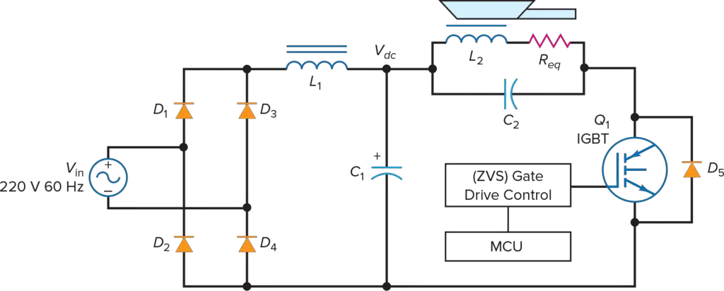
Figure 4. Single-ended (SE) resonant inverter
Solution
The simplified schematic diagram of Figure 4 is a single-ended (SE) resonant inverter. It can be used in induction heating (IH) applications for efficient energy use. This type of inverter can be found in electric home appliances such as stoves, rice cookers, and inverterized microwave ovens. So how does this circuit work?
The 220-Vac input is rectified by the bridge rectifier diodes D1-D4. L1 and C1 form a low-pass, choke-input filter. At the output of the filter is the required dc voltage for the inverter. The primary coil of L2, with its equivalent dc resistance Req, and C2 create a parallel resonant tank circuit. L2 also serves as the primary heating coil winding of a transformer. The secondary of this transformer and its load is a ferrous metal element with low resistance and high permeability. This load essentially works as a one-turn secondary winding with a shorted load and becomes the cooking or heating surface.
Q1 is an IGBT with fast switching speeds, low VCEsat, and high blocking voltage. D5 can either be a copackaged anti-parallel diode or an intrinsic body-diode. The gate of the IGBT is connected to a gate drive control circuit. The gate drive circuit is normally under the control of a microcontroller unit (MCU).
When Q1 receives a proper gate input signal, it turns on ‘allowing current to flow through L2 and the collector to the emitter of the IGBT. The current flow through the primary of L2 creates an expanding magnetic field’ which cuts across the secondary heating element load winding. When Q1 turns off, the energy stored in the magnetic field of L2 collapses and charges up C2. This creates a high positive voltage on the collector of Q1, which uses its high blocking voltage ability to remain off. C2 will return its energy by discharging through L2 in the opposite direction, creating a parallel resonant oscillating current. The expanding and collapsing magnetic field of L2 cuts across the load element. Normally, heat losses as a result of eddy currents are reduced by using laminations. Because the load element does not use laminations, this heat loss can be turned into productive heat energy. This is the principle of IH. To increase the effectiveness of this inductive heating process, the values of L2 and C2 are chosen to create a resonant frequency from 20 to 100 kHz. The higher the frequency of the coil current, the more intense the induced current flowing around the surface of the load, called skin-effect.
The efficiency of this resonant inverter is critical. One of the major power losses of this circuit is the switching losses of the IGBT. Higher energy conversion efficiency is obtained by controlling the IGBT’s voltage or current at the moment of switching. This is known as soft-switching. The voltage or current applied to the switching circuit can be made approximately zero by using the resonance created by the LC resonant circuit and the anti-parallel diode across the collector to the emitter of the IGBT. Gate switch control from the MCU has the voltage of the switching circuit VCE set to zero right before the circuit is turned on (ZVS) and has the IGBT current flow close to zero (ZCS) right before turning it off.
Maximum power is delivered to the load element when the gate drive signal is at the resonant frequency of the LC tank circuit. By regulating the frequency and duty cycle of the gate drive, the temperature of the load can be controlled.
Key Takeaways
Insulated-Gate Bipolar Transistors (IGBTs) play a crucial role in modern electronics, particularly in high-power switching applications. Their unique combination of fast switching speeds and low conduction losses makes them essential components in a wide range of devices and systems, including induction heating appliances, motor control systems, and power converters. By harnessing the advantages of both MOSFETs and BJTs, IGBTs enable efficient energy conversion, improved performance, and enhanced reliability in various industrial and consumer electronics applications.