This article introduces the AVR ATmega328P microcontroller, outlining its architecture, pin layout, packaging options, block diagram, clock sources, and key on-chip peripherals. It also explains programming methods, Arduino integration, digital and analog I/O operations, timers, EEPROM, watchdog functionality, and reset mechanisms to provide a practical understanding of how the Microcontroller Unit (MCU) operates in embedded systems.
What is an ATmega328P Microcontroller?
Microchip manufactures several families of microcontrollers. These include the 8-bit megaAVR family, the 8/16-bit AVR XMEGA family, and the 32-bit AVR UC3 family. This article will focus on the ATmega328P, an 8-bit megaAVR microcontroller, which is the microcontroller used in the popular Arduino Uno microcontroller. Table 1 shows some of the many microcontrollers that are currently available in the megaAVR family, along with some pertinent data on them. The table also lists in parentheses the applicable Arduino board that uses these MCUs.
Note that due to market forces, these microcontrollers are continually replaced by ones with improved features. The letter ‘P’ (which stands for pico power) in the microcontroller part number (such as ATmega48P) specifies an MCU with lower power consumption than the same MCU without the letter ‘P’.
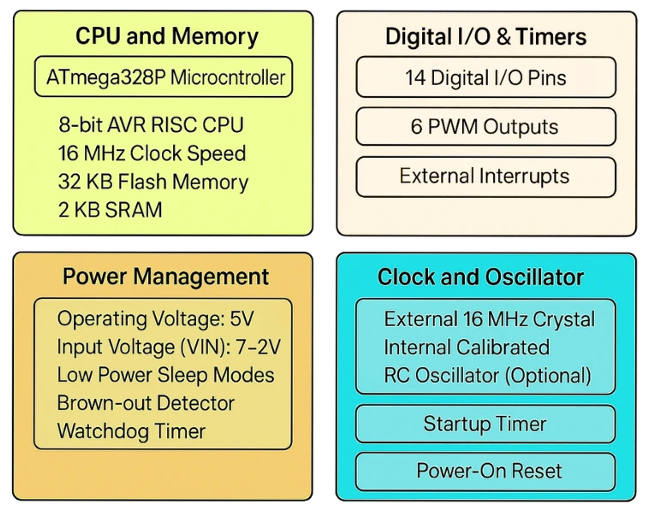
Figure. ATmega328p Microcontroller Key Features
Table 1. A Sampling of Different Microchip MegaAVR Microcontrollers
| AVR MCU (Arduino Board) | Program Memory (Kbytes) | Data EEPROM | RAM | Max I/O | ADC Chan | ADC Bit | PWM Chan | Pin Count | Max Oper. Freq (MHz) | Interface |
| ATmega48P | 4 | 256 | 512 | 23 | 8 | 10 | 6 | 32 | 20 | UART, SPI, I2C |
| ATmega328P (Uno) | 32 | 1024 | 2048 | 23 | 8 | 10 | 6 | 32 | 20 | UART, SPI, I2C |
| ATmega32U4 (Leonardo or Micro) | 32 | 1024 | 2.5 K | 26 | 12 | 10 | 7 | 44 | 16 | UART, SPI, I2C |
| ATmega2560 (Mega 2560) | 256 | 4096 | 8 K | 86 | 16 | 10 | 15 | 100 | 16 | UART, SPI, I2C |
The maximum number of I/O lines refers to the number of digital input/digital output lines available on the chip. These I/O lines are bi-directional and are configured by program code to be either an input or output type.
All the above chips come with analog-to-digital converter capability with a 10-bit resolution. The A/D channels use the same pins as those used for digital I/O lines, but they can be configured by program code to operate as A/D channels.
All the above chips have several PWM lines that can be conveniently used to drive motors through an H-bridge driver or a transistor. The pin count refers to the number of physical pins on the chip. Some chips are available in different pin counts depending on the chip packaging configuration. For example, the ATmega328P MCU is available with 28 pins in the PDIP configuration and with 32 pins in the TQFP configuration.
The maximum operating frequency refers to the maximum speed of the clock that can drive the chip. The chips listed in Table 1 have a maximum clock frequency of 20 MHz or lower. All the listed chips have interfaces for ease of communication with other devices. An explanation of these interfaces is given in Table 2.
Table 2. A List of Interfaces Available on Some MCUs
| Interface Feature | Explanation |
| USART | Universal Synchronous Asynchronous Receiver Transmitter (USART) module—used for synchronous (data line and clock signal) and asynchronous (data line but no clock signal) serial communication |
| AUSART | Addressable Universal Synchronous Asynchronous Receiver Transmitter (AUSART) module—Can be configured as Asynchronous (full duplex), Synchronous—Leader (half duplex), or Synchronous—Follower (half duplex) serial communication line |
| EUSART | Enhanced Universal Synchronous Asynchronous Receiver Transmitter (EUSART) module—Supports RS-485, RS-232, and LIN compatibility—Auto-Baud Detect—Auto-wake-up on Start bit |
| MSSP | Leader Synchronous Serial Port (MSSP) module, which includes an SPI™ and I2C™ |
| SPI™ | Synchronous serial port configured as 3-wire Serial Peripheral Interface (SPI™) |
| I2C™ | Synchronous serial port configured as a 2-wire Inter-Integrated Circuit (I2C™) bus |
| USB | Universal Serial Bus |
| LIN | Local Interconnect Network, which is a serial communication system |
ATmega328P Pinout
MCUs are available in different pin layouts (see Figure 1).
- A common layout is the PDIP (Plastic Dual Inline Package). In this layout, the pins are arranged in two parallel opposite rows, and this layout is normally used with breadboards.
- The SOIC (Small-Outline Integrated Circuit) layout uses gull-wing pins extending outward that are more tightly spaced than the PDIP.
- The QFP layout (Quad-Flat Package) has pins on all four sides of the package, while the QFN (Quad-Flat No-Leads) layout also has pins on all four sides, but the pins are exposed on the bottom and sometimes on both sides and the bottom. QFP and QFN layouts are also available in other variations, including thin QFP (TQFP), low-profile QFP (LQFP), or very-thin QFN (VQFN).
Integrated circuits in SOIC, QFP, and QFN layouts are classified as surface-mount-type devices. These layouts are not designed to be used on breadboards, and special automated tools are used to solder these chips to circuit boards.
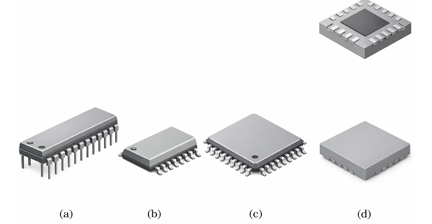
Figure 1. (a) PDIP, (b) SOIC, (c) QFP, and (d) QFN packaging
Figure 2 shows the pin layout for the ATmega328P MCU in the PDIP configuration. The ATmega328P has three I/O ports labeled PB, PC, and PD. Because this MCU has only 28 pins but supports many interface functions, many of the pins are designed for more than one function.
For example, pin 23 can be configured as channel 0 of digital input/output port C (PC0), analog-to-digital converter channel 0 (ADC0), or pin change interrupt 8 (PCINT8). The limited number of external pins also means that you cannot have 8 A/D channels and 23 I/O lines operating at the same time. Table 3 explains the labels of these pins.
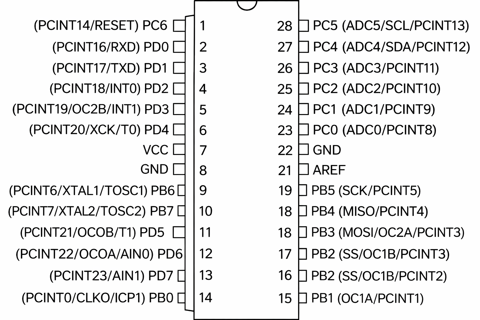
Figure 2. Pin layout for ATmega328P Microcontroller
Table 3. Pin Functions on ATmega328p MCU
| ADC | Analog-to-digital converter input channel |
| AIN0 | Analog comparator positive input |
| AIN1 | Analog comparator negative input |
| AREF | External voltage reference for A/D |
| AVCC | Supply voltage pin for A/D |
| CLKO | Divided system clock output |
| ICP1 | Timer/counter 1 input capture pin |
| INT | External interrupt input pin |
| GND | Ground reference line |
| MISO | SPI bus leader input/follower output |
| MOSI | SPI bus leader output/follower input |
| OC0A, OC1A, OC2A | Timer/counter (0, 1, and 2) output compare match A output |
| OC0B, OC1B, OC2B | Timer/counter (0, 1, and 2) output compare match B output |
| PB, PC, PD | Digital input/output ports B, C, and D |
| PCINT | Pin change interrupt |
| RESET | Reset pin |
| RXD | USART input pin |
| SCK, SCL | SPI clock, and I2C clock |
| SS | Follower select line for SPI |
| T0, T1 | Timer/counter0 (or 1) external counter input |
| TOSC | Timer oscillator pin |
| TXD | USART output pin |
| VCC | Positive lead of the supply voltage. This chip operates at an input voltage range of 1.8-5.5 V |
| XCK | USART external clock input/output |
| XTAL | Chip clock oscillator pin |
ATmega328P AVR Microcontroller Block Diagram
Figure 3 shows a block diagram of the main components of the ATmega328P MCU. Some of these components include:
- three digital I/O ports (Ports B, C, and D)
- three timers/counters (T/C 0, 1, and 2)
- USART module for RS232 communication
- A/D converter module
- SPI and I2C module
- lash program memory
- SRAM
- CPU
Note how the 8-bit data bus connects the CPU to the other components on the MCU.
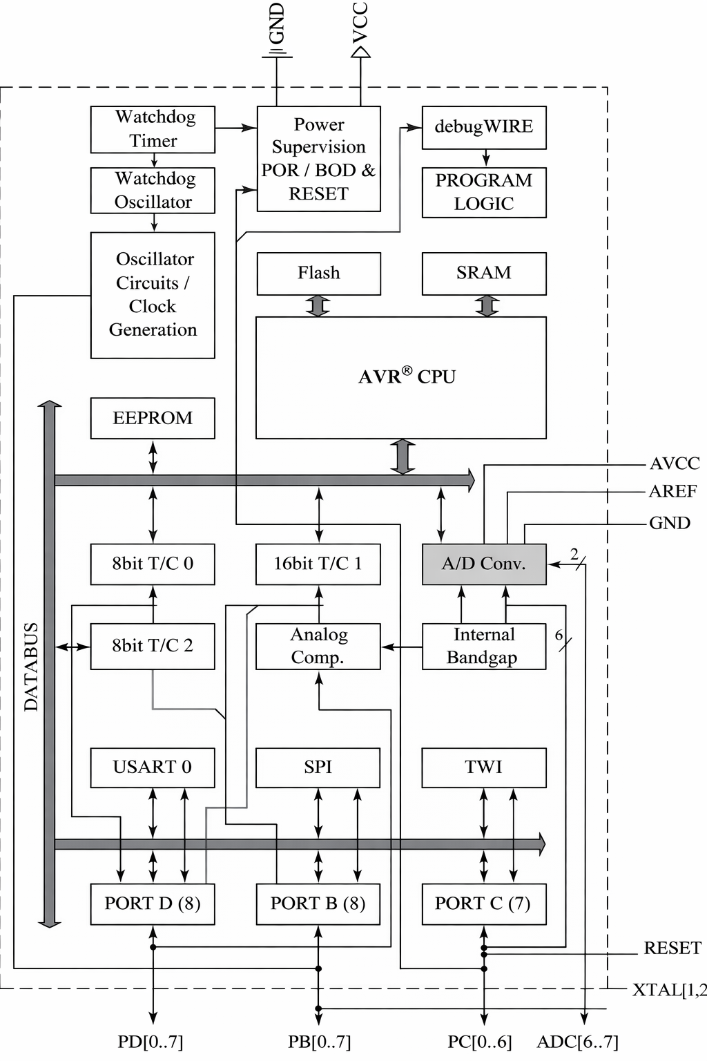
Figure 3. A block diagram of the ATmega328P Microcontroller
Arduino Uno Board
The Arduino Uno board is an open-source MCU-based development platform that includes an AVR ATmega328P MCU built into the board. The Arduino boards were first introduced in 2005. Since then, there have been several boards available, including the famous Arduino Uno, Arduino Leonardo, and Arduino Nano.
While the different Arduino boards have different sizes and memories, they all share a nearly similar board structure and labeling. The Arduino boards have attracted the attention of many users due to the freely available software to program the boards, the ease of connecting wires to the boards, and the ease of connecting the boards to a computer.
In addition, the boards take advantage of the large availability of shields, which are interchangeable custom boards that are mounted on the top of the Arduino boards to provide additional functionality such as prototyping, Ethernet communication, or motor drive.
A picture of the original Arduino Uno R3 board is shown in Figure 4. There have been several revisions of the Uno board, and the one shown in the figure is revision three or R3. The original boards refer to the ones made by the Arduino consortium in Italy.
Note that since the Arduino boards are open source, many companies make similar boards that are usually less expensive than the original ones. The Arduino Uno board has two AVR Microcontrollers. It has an ATmega328P MCU as the main MCU, which is available for the user to program, and an ATmega16U2, which is solely used for communication between the board and a PC.
In addition to these two MCUs, the board has additional components. These include:
- 16 MHz crystal oscillator
- 16 MHz ceramic resonator
- various connectors
- LEDs
- Reset switch
The board connects to a computer via a Type A/B USB cable. The board operates at a 5 VDC voltage level and could be powered by an adapter that supplies 7-12 VDC. The board can also operate on the power provided to it by the USB cable, but the cable can only provide a maximum current of 500 mA to the board.
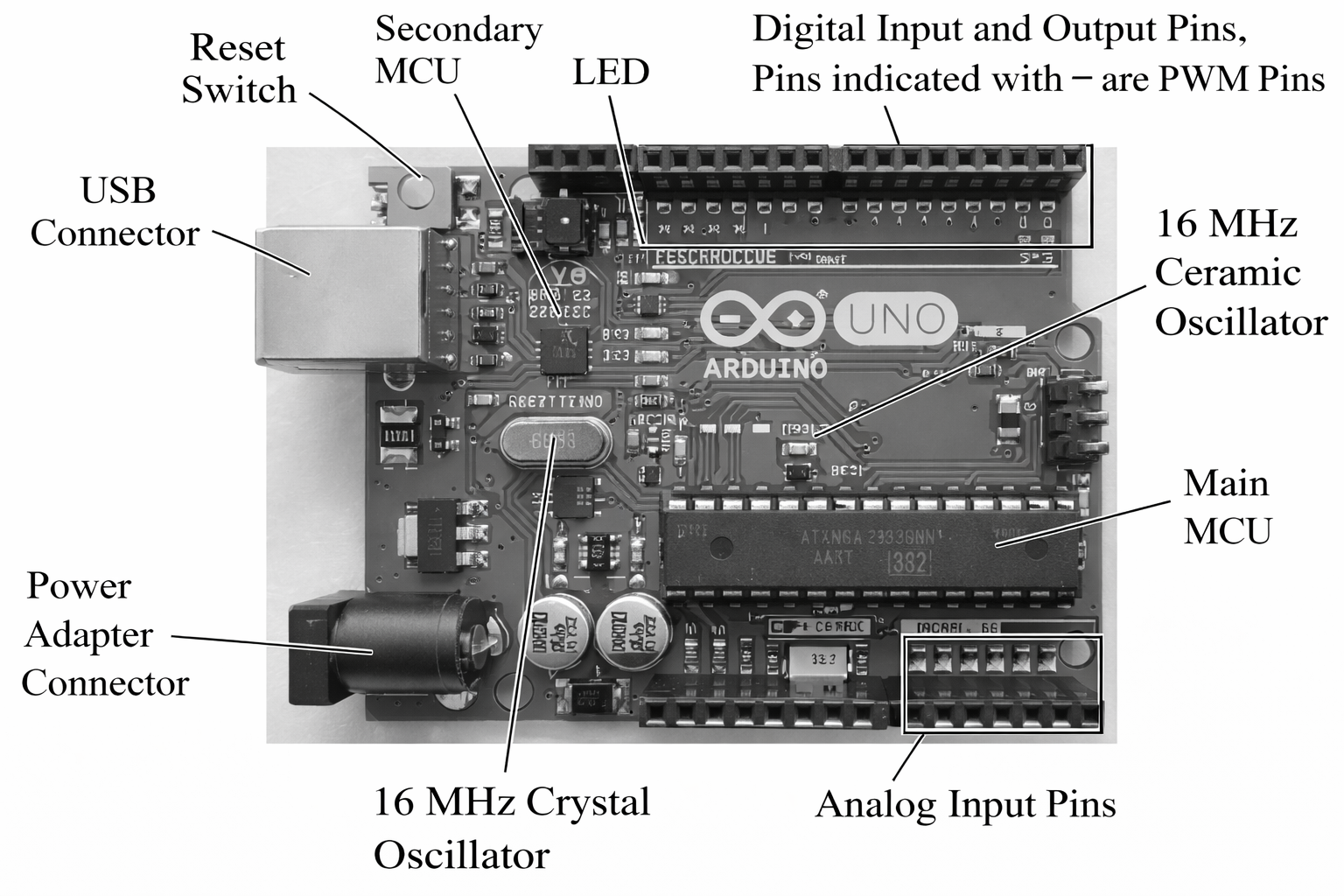
Figure 4. Top view of the Arduino Uno R3 board
Note that the pin numbers shown on the boards are different from the pin numbers on the ATmega328P chip. The correspondence between the pin numbers is shown below in Table 4.
Table 4. Correspondence between Pin Numbers on the Arduino Uno Board and the ATmega328P Chip
| Pin # on Uno | ATmega328P Port | Function |
| Analog A0 | PC0 | Analog Input |
| Analog A1 | PC1 | Analog Input |
| Analog A2 | PC2 | Analog Input |
| Analog A3 | PC3 | Analog Input |
| Analog A4 | PC4 | Analog Input, I2C SDA |
| Analog A5 | PC5 | Analog Input, I2C SCL |
| Digital 0 | PD0 | Digital I/O, USART RXD |
| Digital 1 | PD1 | Digital I/O, USART TXD |
| Digital 2 | PD2 | Digital I/O |
| Digital 3 | PD3 | Digital I/O, PWM T2 |
| Digital 4 | PD4 | Digital I/O |
| Digital 5 | PD5 | Digital I/O, PWM T0 |
| Digital 6 | PD6 | Digital I/O, PWM T0, Analog Comparator positive input |
| Digital 7 | PD7 | Digital I/O, Analog Comparator negative input |
| Digital 8 | PB0 | Digital I/O, Input Capture |
| Digital 9 | PB1 | Digital I/O, PWM T1 |
| Digital 10 | PB2 | Digital I/O, PWM T1, SPI SS |
| Digital 11 | PB3 | Digital I/O, PWM T2, SPI MOSI |
| Digital 12 | PB4 | Digital I/O, SPI MISO |
| Digital 13 | PB5 | Digital I/O, SPI SCK |
An advantage of Arduino boards is that they can be programmed without the need for an external programmer. The Arduino environment software has this feature built into it, and it allows the user to upload the code to the MCU by simply clicking on a button.
Clock/Oscillator Source
A microcontroller needs a clock source to function since all CPU operations are synchronized with the clock. A clock is any device that can produce a train of pulses at a fixed frequency. Most of these devices are called oscillators, which is the term given to an electronic circuit that uses a DC power source to generate a periodic AC signal.
Some MCUs have a built-in clock source while others require or allow an external device to produce the clock pulses. The ATmega328P also has two internal oscillators: an 8 MHz high-frequency oscillator and a 128 kHz low-frequency oscillator, but it also allows the use of an external clock source.
The output frequency of the internal 8 MHz oscillator can be further divided by software. The effective clock frequency of an internal oscillator varies with the supply voltage and the temperature of the MCU.
External devices to produce a clock signal include a quartz crystal resonator, a ceramic resonator, a resistor-capacitor (RC) oscillator circuit, or an external clock source such as the 555-timer chip. The microcontroller allows through software the selection of the clock source.
A quartz crystal resonator uses the mechanical resonance of a piezoelectric crystal to generate a very accurate timing signal while a ceramic resonator uses the mechanical resonance of piezoelectric ceramics (commonly Lead Zirconate Titanate or PZT). Ceramic resonators are small, rugged, and inexpensive, while quartz crystal resonators are more expensive but more precise.
Ceramic and quartz crystal resonators are available with different clock frequencies. A photo of a quartz crystal resonator is shown in Figure 5(a), while that of a ceramic resonator is shown in Figure 5(b).
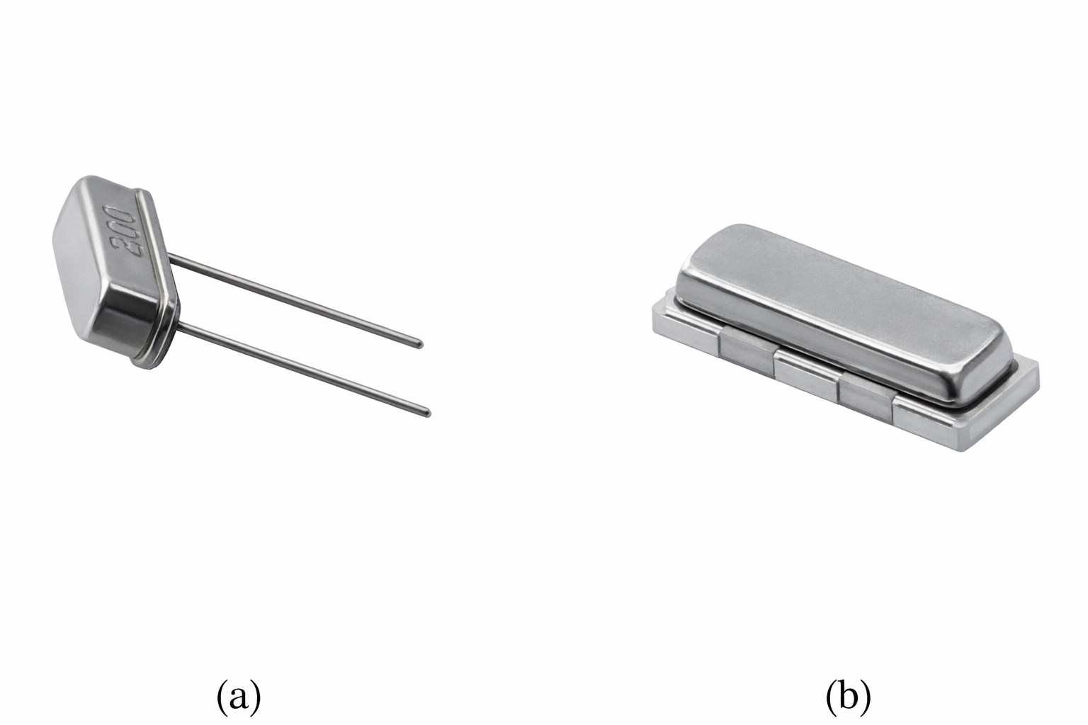
Figure 5. (a) A quartz crystal resonator and (b) a ceramic resonator
An RC oscillator circuit uses a feedback network of three RC circuits arranged in a ladder fashion and connected to a BJT transistor or an inverting Op-amp to produce a clock signal. It is normally used in applications where clock accuracy (1-10% error) is not very important.
An external clock source, such as the 555 timer, can also be used as the clock. A 555-timer chip (such as the NE555 8-pin chip from Texas Instruments) is an integrated circuit that uses transistors, resistors, and diodes to produce a variety of clock signals, including periodic signal output and time delays.
The Arduino Uno board uses a 16 MHz ceramic resonator as the clock source for the primary MCU (ATmega328P). Since a ceramic resonator is not very precise (accuracy is about 0.5%), the Arduino Uno board should not be used for precision timing applications since it could produce a timing error of about 18 seconds over an hour of operation.
The board also uses a 16 MHz external crystal oscillator as the clock source for the secondary MCU (ATmega16U2), which is solely used for USB/serial communication between the board and a PC. USB communication is very sensitive to clock signal accuracy, which is why the high-precision crystal oscillator (accuracy of 0.003%) is used for timing the operation of the secondary MCU. Figure 4 shows these devices on the Uno board.
To get an MCU to run, at least three pins need to be wired. These include:
- Power supply pin (VCC pin on AVR MCUs), which should be connected to the positive lead of the supply voltage (1.8 to 5.5 volts for most AVR chips)
- Ground pin (GND pin on AVR MCUs,) which should be connected to ground voltage
- Reset pin (RESET pin on AVR MCUs,) which needs to be connected to the supply voltage (through a resistor) to prevent the MCU from resetting itself.
For microcontrollers without internal clock sources, you also need to connect the external clock source to the microcontroller.
Programming a Microcontroller
The development of a control program running on a microcontroller has similarities to developing a program to run on a PC. In both cases, high-level programming languages such as C or Python are often used to write the code.
Within a development environment, which may be tailored to a specific language or microcontroller, the high-level code is compiled into binary code using the built-in compiler. This binary code is then linked with other necessary files to form the executable program.
On a PC, this program can be run simply by calling its name, while on a microcontroller, the compiled code must typically be loaded onto the device. In both cases, the development environment often includes debugging tools that allow developers to identify and correct errors in the code. This approach helps streamline the development process, whether targeting a traditional computing platform or an embedded microcontroller system.
In microcontroller development, programmers have the option to use either high-level programming languages such as C or low-level assembly language. Assembly language is tailored specifically to the architecture of the microcontroller being used. Though programming in assembly can be more challenging, it offers greater control over the execution timing of the code, as the number of clock cycles needed to execute each instruction is known. This allows for precise control and optimization of performance.
Another benefit of using assembly language is the typically cost-free availability of assembly compilers, as they are often provided without charge by the microcontroller manufacturer or other sources.
Whether using high-level or assembly language, the code must be compiled and translated into binary code (or a hex code file). This binary or hex code is then downloaded to the microcontroller, where it is stored in the non-volatile program memory, ready for execution. This dual approach of using either high-level languages or assembly offers flexibility to developers, balancing ease of use and powerful, fine-grained control.
One appealing feature of Arduino boards is the free Integrated Development Environment (IDE) software used to program them. The IDE is a combination of a text editor for writing and editing code and a compiler to validate the code’s syntax and convert it into binary code that the Microcontroller Unit (MCU) can read.
With Arduino boards, the user simply connects a USB cable between the board and a PC or laptop, then uses commands within the IDE to compile and upload the program (referred to as a ‘sketch’ in Arduino terminology) to the microcontroller.
The Arduino IDE employs a built-in boot-loading application, eliminating the need for an external programmer. A bootloader application is a special piece of software that facilitates the process of loading the operating system or other necessary programs (known as the ‘boot image’) into a device’s memory. In the context of microcontrollers, a bootloader is a small program that resides in a dedicated section of the device’s memory, and its primary function is to load the main application code.
AVR Microcontrollers support boot loading because their program memory is divided into two sections: one for program instructions and the other (located at the upper end of program memory) for the boot loading section, where the bootloader code resides.
- When the microcontroller is powered on or reset, the bootloader is the first program that runs. It checks whether there is a new version of the application code to be loaded, usually communicating with an external source like a PC via a specific protocol (such as serial communication).
- If new code is present, the bootloader loads it into the appropriate area of the microcontroller’s memory, overwriting the existing application code if necessary.
- The bootloader then passes control to the main application, which begins executing.
Bootloaders are especially useful in embedded systems, where updating the software might be more challenging than in a typical computer environment. By providing a controlled way to load new code onto the device, bootloaders enable updates, bug fixes, and feature enhancements to be applied without requiring specialized hardware or physical access to the device. The complete process of programming a microcontroller, including these steps, is illustrated in Figure 6.
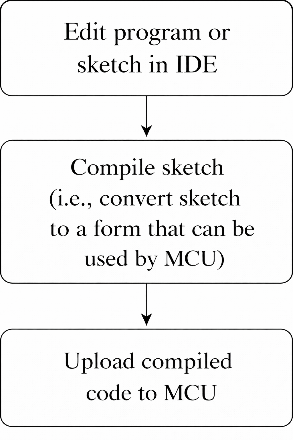
Figure 6. Process of programming a microcontroller
Digital Input/Output and Analog-to-Digital Conversion Operations
One of the basic operations that an MCU does is digital input and digital output. This is used when a microcontroller needs to interface with external devices such as switches, relays, and lights. A digital input operation reads an input voltage signal and converts it into one of the two digital logic levels, while a digital output operation takes a logic signal (either high or low) and converts it into an output voltage level.
The low and high logic values correspond to different voltages depending on the construction family of the microcontroller. The Arduino MCU is built using the CMOS family. However, it has slightly different voltage level ranges than a standard CMOS. Figure 7 shows the voltage levels for the Arduino Uno MCU using a 5 V supply voltage. The values define the allowable voltage ranges for the low and high logic states.
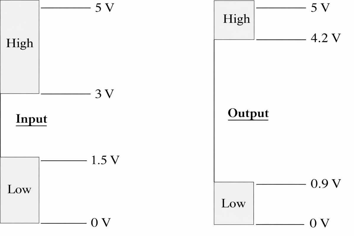
Figure 7. Input and output voltage levels for Arduino Uno
While the ATmega328P MCU has a maximum of 23 pins that can be used for digital I/O, the Arduino Uno board makes available to the user a maximum of 14 pins (pins 0 through 13) that can be used for digital input and output operations (see Figure 4).
Pins 0 and 1 will not operate properly if serial communication is active during program execution, as these two pins are used for serial communication between the MCU and the PC. Each of the digital I/O pins can be used for either input or output. If the direction is not explicitly set, the input/output pins on the Arduino default to input.
Arduino provides a function that can be used to configure the pins. The function is called pinMode() and is listed below, where pin is the pin number, such as 3 or 8, and mode is either OUTPUT, INPUT, or INPUT_PULLUP.
pinMode (pin, mode)—Configures the specified pin to behave either as an input, an output, or an input with pull-up mode activated.
Without using the Arduino-provided pin configuration function, the user must write code to configure the data direction register associated with the port to which the pin belongs. For example, the ATmega328P has three I/O ports referred to as ports B, C, and D, and three data direction registers associated with these ports and referred to as DDRB, DDRC, and DDRD, respectively.
On the AVR Microcontroller, a value of 1 written to the data direction register bit corresponding to a particular I/O pin causes that pin to function as a digital output, while a value of zero causes that pin to function as a digital input.
The Arduino pin configuration function can also be used to configure a pin as an input with a special mode of operation called pull-up mode. The special mode makes use of a built-in 20 kΩ pull-up resistor that is attached to each I/O pin. The primary purpose of the pull-up resistor is to steer the input pin to a known state when no input is present.
As seen in Figure 8, when the pull-up resistor is activated and the switch is open, the input pin voltage will be close to VCC. When the switch is closed, current flows through the pull-up resistor to the ground, and the voltage at the input pin will be zero. There is a chance for the input to float, which could cause fluctuation in the reading if this mode is not used and no input signal is connected to the pin.
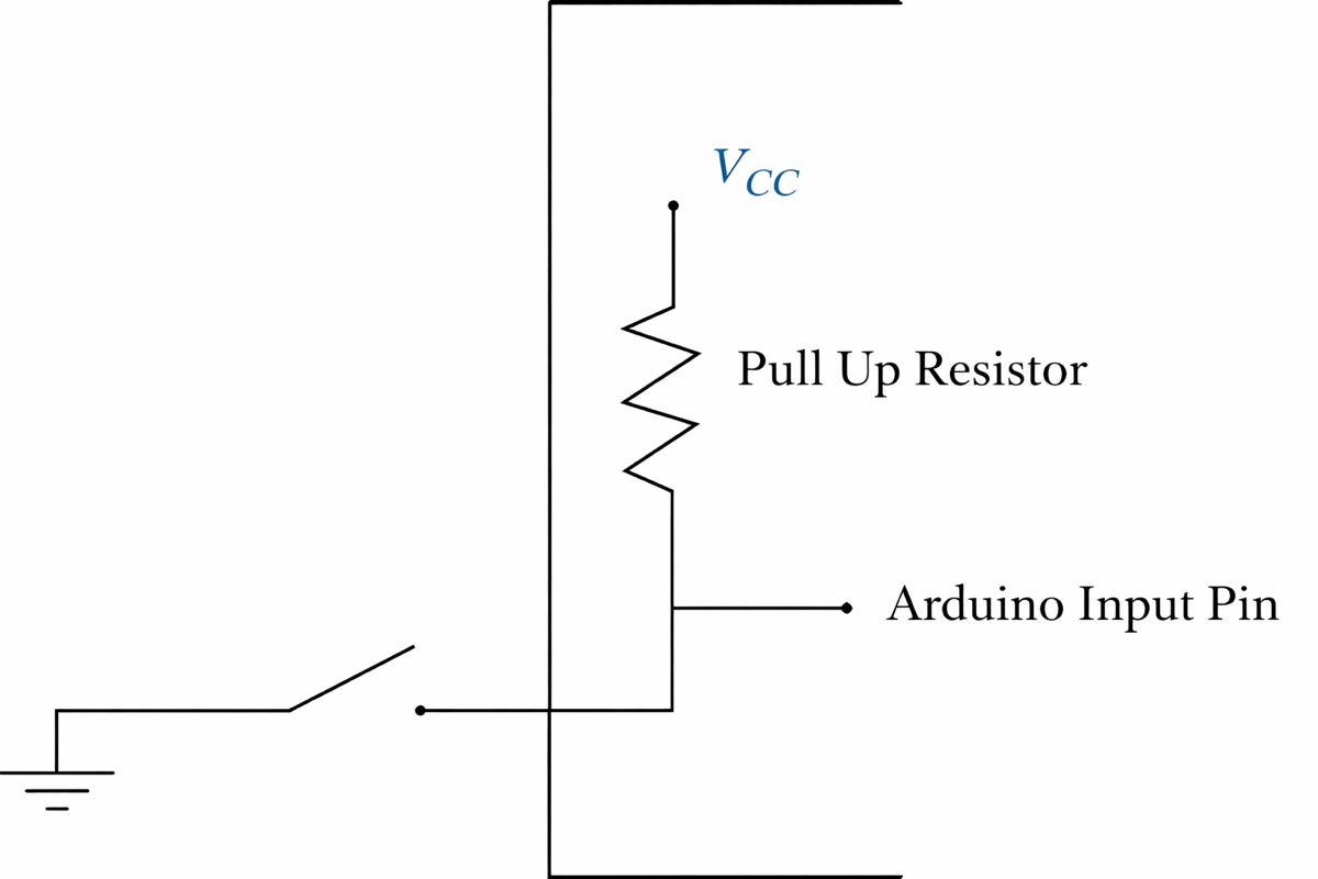
Figure 8. Pull-up resistors on AVR I/O pins
To read or send digital values, Arduino provides the following two functions:
- digitalWrite (pin, value)—Write a HIGH or a LOW value to a digital pin
- digitalRead (pin)—Reads the value from a specified digital pin
Many MCUs, including the ATmega328P, can convert an analog voltage to a digital value through a device called an analog-to-digital (A/D) converter. An A/D converter is used to read the output from analog sensors such as potentiometers and tachometers.
An A/D converter performs a mapping operation between analog voltages (such as between 0 and 5 volts) and a set of digital values (such as between 0 and 1023) similar to how an instructor maps numerical grades between 0 and 100 to a set of specific letter grades (such as 94 to 100 is mapped to A, 90 to 93 is mapped to A-, … etc.).
- The analog voltage range that is mapped is typically between 0 volts and the supply voltage to the MCU (called either VCC or VDD), but a different range can be used if an external voltage was used as the reference signal (connected to the AREF pin on AVR MCUs).
- The set of digital values is a function of the resolution of the A/D converter. On the ATmega328P, the resolution is 10 bits, which means that the analog voltage range is mapped into 1024 (or 210) values.
The Arduino Uno board has six channels dedicated to A/D conversion that are labeled channels A0 through A5 on the board (see Figure 4). Arduino provides the analogRead(pin) function to read the analog voltage applied to these pins, where pin is the analog pin number (0 to 5 on the UNO board). It takes approximately 0.1 ms to do a single A/D conversion.
AVR Microcontroller Components and Features
In this section, we will discuss several components and features of AVR MCUs. These include EEPROM data, delays and timers, watchdog timer, and reset operations.
EEPROM Data
The EEPROM (Electrically Erasable Programmable Read-Only Memory) is a type of non-volatile memory that can be used to store data in embedded systems, including Arduino-based platforms. Unlike RAM (Random Access Memory), where data is lost when power is removed, data stored in EEPROM remains intact even when the device is turned off.
The data in EEPROM can be written either during the programming phase or while the program is executing. Writing data to EEPROM during program execution takes longer than writing to a RAM location, but the advantage is that the data is permanently stored.
The Arduino development environment provides a standard library, known as ‘EEPROM,’ with functions that enable easy access to the EEPROM memory. These functions include:
- EEPROM.read(address): This function reads the data stored in EEPROM at the specified memory address. It is used to retrieve data that has been previously stored, allowing for persistent data storage between power cycles or resets.
- EEPROM.write(address, value): This function erases the existing data at the specified memory address and writes the new value to the EEPROM. This enables the modification of stored data, and since EEPROM has a finite number of write cycles (often around 100,000), the erasing and rewriting should be done judiciously.
In the context of real-world applications, EEPROM is often utilized to store configuration settings, calibration data, user preferences, or any information that needs to be retained after a power loss. It provides a small but reliable storage solution where data persistence is essential, even though the access times are longer compared to RAM.
Timing Delays and Timers
The Arduino development environment provides two functions for timing delays. These are delay() and delayMicroseconds().
- The maximum delay interval that can be set with the delay() function is around 50 days (set in millisecond units), but this value may vary depending on the Arduino board being used.
- The delayMicroseconds() function allows more precise delays as the delay is set in microsecond units, but the maximum delay interval for this function is about 70 minutes.
These functions are typically used for creating a simple time delay between different parts of a program, and they work by executing a precise number of instructions to cause the requested delay. They do not use any timers.
An important consideration when using these delay functions is that other code execution (except for interrupt service routines) is blocked during the delay. This means that if you have tasks that need continuous monitoring or frequent updates, using these functions may lead to unresponsive behavior.
For more advanced timing control, such as measuring time intervals between events, tracking the occurrence of an event relative to another point in the code, or creating non-blocking delays, it may be necessary to access timers directly.
The ATmega328P has three timers referred to as Timer0, Timer1, and Timer2. Timer1 uses a 16-bit counter while Timer0 and Timer2 use 8-bit counters. Some of these timers can operate as either timers or counters.
- In the timing mode, the count value is incremented every clock cycle or at a multiple of it if a prescaler is used, where a prescalar is a user-set factor that can divide the input clock frequency for that timer.
- In the counter mode, the timer module will increment on every rising or falling edge of the external signal connected to the microcontroller. The user has a choice of setting the clock source for these timers, as well as setting the maximum overflow interval.
All the above timers can use a prescaler. Having a prescale factor higher than 1:1 increases the maximum counting interval before the counter overflow. Example 1 illustrates the use of the prescale factor.
Example 1: Timer Counting Interval
Using an 8 MHz internal clock, and 1:8 prescale factor, determine the maximum counting interval for Timer1 on the ATmega328P.
Solution
The input clock frequency to Timer1 would be 1 MHz (1/8 × 8) or a counter resolution of 1 μsec. Since Timer1 is associated with a 16-bit counter, the maximum counting interval is $ 2^{16}\times 1\mu sec=65536\mu sec$ or 65.53 ms. Thus, with an 8:1 prescale factor, the Timer1 counter will overflow once every 65.53 ms.
Watchdog Timer
The watchdog timer (WDT) is a special counter that resets the processor if it overflows. The purpose of the WDT is to cause the processor to reset if it times out in a lengthy operation. To prevent overflow, the program needs to periodically reset the counter associated with the watchdog timer.
The MCU’s hardware handles the WDT, independent of any program running on the MCU. In the AVR MCU, the WDT is controlled by the WDTCSR (Watchdog Timer Control) register. The watchdog timer uses a dedicated internal low-frequency clock running at 128 kHz for its timing functions, which is independent of the internal high-frequency oscillator clock. The overflow period is processor-dependent, and on the ATmega328P, the overflow period can range from 16 ms to 8 seconds.
In addition to resetting the processor, the WDT on the AVR Microcontroller can also cause an interrupt or both actions simultaneously. If the WDT is enabled in the code, then the user program should include a call to periodically reset the counter associated with the watchdog timer.
If the code was stuck in a code segment for an interval longer than the WDT overflow period, there is no chance to restart the WDT before it overflows, and the WDT will keep resetting (i.e., causing the program to start from the beginning).
Reset Operations
There are different reset operations in AVR Microcontrollers. These include Power-on Reset (POR), Brown-out Reset (BOR), Watchdog Timer Reset, and External Reset.
- A POR occurs whenever the power (Vcc line) is turned off and then on to the chip. After a POR, the code on the chip starts executing from the instruction placed at the reset vector address, and the I/O lines and some of the registers on the chip will reset to their ‘Reset’ state.
- A BOR (if enabled) produces the same result as a POR and occurs whenever the VCC voltage level falls below the rated voltage (between 1.8 and 5.5 volts for most chips). The BOR does not occur unless certain registers on the chip were set to detect this condition. This feature is useful in battery-powered applications to detect low-voltage conditions.
- The Watchdog Timer Reset occurs whenever the counter associated with the WDT overflows, while an External Reset occurs whenever the reset pin (the RESET pin on AVR MCUs) goes to low for a certain minimum interval.
Note that the MCU has a special register that can indicate which type of reset has occurred. In AVR MCUs, it is called the MCUSR (MCU Status Register).
Review Questions?
Name several pin layouts for MCUs.
PDIP (Plastic Dual Inline Package), SOIC (Small-Outline Integrated Circuit), QFP (Quad-Flat Package), and QFN (Quad-Flat No-Leads).
Name three external clock sources.
External clock sources include a quartz crystal resonator, a ceramic resonator, a resistor-capacitor (RC) circuit, or an external clock source such as the 555-timer chip.
What are the minimum connections needed for an MCU to operate?
To get an MCU to run, at least three pins need to be wired. These include the power supply pin (VCC pin on AVR MCUs), which should be connected to the positive lead of the supply voltage (1.8 to 5.5 volts for most AVR chips); the ground pin (GND pin on AVR MCUs), which should be connected to ground voltage; and the reset pin (RESET pin on AVR MCUs), which needs to be connected to the supply voltage (through a resistor) to prevent the MCU from resetting itself. For microcontrollers without internal clock sources, you also need to connect the external clock source to the microcontroller.
How is a Microcontroller programmed?
An AVR Microcontroller, for example, can be programmed using software that is provided in an Integrated Development Environment (IDE) for the MCU or through the use of a boot loader program. A chip is programmed when the hex code is transferred to the program memory area on the chip.
What is a boot-loading application?
A bootloader application is a special piece of software that facilitates the process of loading the operating system or other necessary programs (known as the ‘boot image’) into a device’s memory.
What is the advantage of pull-up mode in digital input operations?
The advantage of the pull-up mode is to steer the input on the digital input pin to a known state when no input is present.
What are the different PWM modes available on the ATmega328P?
The different modes are:
- Fast PWM
- Phase Correct PWM
- Phase and Frequency Correct PWM
Which PWM mode offers the highest frequencies?
Fast PWM mode offers the highest frequencies.
What is the limitation of the use of the delay() function?
A limitation of the delay() function is that other code execution (except for interrupt service routines) is blocked during the execution of this function.
What is the advantage of storing data in EEPROM Data memory?
Data cannot be lost even when the MCU has lost power.
What is the purpose of a watchdog timer?
The purpose of the WDT is to cause the processor to reset if it times out in a lengthy operation. To prevent overflow, the program needs to periodically reset the counter associated with the watchdog timer.
What happens after a Power-on reset?
After a Power-on reset, the code on the chip starts executing at the first program memory instruction, and some of the registers on the chip will reset to their “Reset” state.
Key Takeaways
Understanding the architecture, peripherals, and programming model of the ATmega328P and related AVR microcontrollers is essential for designing reliable and efficient embedded systems. Features such as flexible digital and analog I/O, built-in ADC, timers, PWM modules, EEPROM, watchdog functionality, and multiple communication interfaces enable these MCUs to support applications ranging from simple sensor-based control systems to motor drives, data acquisition units, and IoT prototypes. When combined with accessible development platforms like Arduino, these capabilities lower the barrier to rapid prototyping while still providing the depth and control required for industrial, educational, and commercial embedded solutions.